The Xeon E5-2600: Dual Sandy Bridge for Servers
by Johan De Gelas on March 6, 2012 9:27 AM EST- Posted in
- IT Computing
- Virtualization
- Xeon
- Opteron
- Cloud Computing
Benchmark Configuration
Unfortunately, the Intel R2208GZ4GSSPP is a 2U server, which makes it hard to compare it with the 1U Opteron "Interlagos" and 1U "Westmere EP" servers we have tested in the past. We will be showing you a few power consumption numbers, but since a direct comparison isn't possible, please take them with a grain of salt.
Intel's Xeon E5 server R2208GZ4GSSPP (2U Chassis)
| CPU |
Intel Xeon processor E5-2690 (2.9 GHz, 8c, 20MB L3, 135W) |
| RAM | 64 GB (8x8GB) DDR-1600 Samsung M393B1K70DH0-CK0 |
| Motherboard | Intel Server Board S2600GZ "Grizzly Pass" |
| Chipset | Intel C600 |
| BIOS version | SE5C600.86B (01/06/2012) |
| PSU | Intel 750W DPS-750XB A (80+ Platinum) |
The Xeon E5 CPUs have four memory channels per CPU and support DDR3-1600, and thus our dual CPU configuration gets eight DIMMs for maximum bandwidth. The typical BIOS settings can be found below.
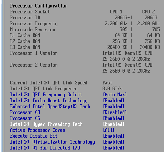
Not being show is that all prefetchers were enabled in all tests.
Supermicro A+ Opteron server 1022G-URG (1U Chassis)
| CPU |
Two AMD Opteron "Bulldozer" 6276 at 2.3GHz Two AMD Opteron "Magny-Cours" 6174 at 2.2GHz |
| RAM | 64GB (8x8GB) DDR3-1600 Samsung M393B1K70DH0-CK0 |
| Motherboard | SuperMicro H8DGU-F |
| Internal Disks |
2 x Intel SLC X25-E 32GB or 1 x Intel MLC SSD510 120GB |
| Chipset | AMD Chipset SR5670 + SP5100 |
| BIOS version | v2.81 (10/28/2011) |
| PSU | SuperMicro PWS-704P-1R 750Watt |
The same is true for the latest AMD Opterons: eight DDR3-1600 DIMMs for maximum bandwidth. You can find the BIOS settings of our Opteron machine here. C6 was enabled.
Asus RS700-E6/RS4 1U Server
| CPU |
Two Intel Xeon X5670 at 2.93GHz - 6 cores Two Intel Xeon X5650 at 2.66GHz - 6 cores |
| RAM | 48GB (12x4GB) Kingston DDR3-1333 FB372D3D4P13C9ED1 |
| Motherboard | Asus Z8PS-D12-1U |
| Chipset | Intel 5520 |
| BIOS version | 1102 (08/25/2011) |
| PSU | 770W Delta Electronics DPS-770AB |
To speed up testing, we tested the Intel Xeon and AMD Opteron system in parallel. As we didn't have more than eight 8GB DIMMs, we used our 4GB DDR3-1333 DIMMs. The Xeon system only gets 48GB, but this isn't a disadvantage as our highest memory footprint benchmark (vApus FOS, 5 tiles) uses no more than 40GB of RAM.
Finally, we measured the difference between 12x4GB and 8x8GB of RAM and recalculated the power consumption for our power measurements (note that the differences were very small). There is no alternative as our Xeon has three memory channels and cannot be outfitted with the same amount of RAM as our Opteron system (four channels).
Common Storage System
For the virtualization tests, each server gets an Adaptec 5085 PCIe x8 card (driver aacraid v1.1-5.1[2459] b 469512) connected to six Cheetah 300GB 15000 RPM SAS disks (RAID-0) inside a Promise JBOD J300. The virtualization testing requires more storage IOPs than our standard Promise JBOD with six SAS drives can provide. To counter this, we added internal SSDs:
- We installed the Oracle Swingbench VMs (vApus Mark II) on two internal X25-E SSDs (no RAID). The Oracle database is only 6GB big. We test with two tiles. On each SSD, each OLTP VM accesses its own database data. All other VMs (web, SQL Server OLAP) are stored on the Promise JBOD (see above).
- With vApus FOS, Zimbra is the I/O intensive VM. We spread the Zimbra data over the two Intel X25-E SSDs (no RAID). All other VMs (web, MySQL OLAP) get their data from the Promise JBOD (see above).
We monitored disk activity and measured the phyiscal disk adapter latency (as reported by VMware vSphere) at between 0.5 and 2.5 ms.
Software Configuration
All vApus testing was done one ESXi vSphere 5--VMware ESXi 5.0.0 (b 469512 - VMkernel SMP build-348481 Jan-12-2011 x86_64) to be more specific. All vmdks use thick provisioning, independent, and persistent. The power policy is "Balanced Power" unless indicated otherwise. All other testing was done on Windows 2008 Enterprise R2 SP1. Unless noted otherwise, we used the "High Performance setting" on Windows 2008 R2 SP1.
Other Notes
Both servers were fed by a standard European 230V (16 Amps max.) powerline. The room temperature was monitored and kept at 23°C by our Airwell CRACs.
We used the Racktivity ES1008 Energy Switch PDU to measure power consumption. Using a PDU for accurate power measurements might seem pretty insane, but this is not your average PDU. Measurement circuits of most PDUs assume that the incoming AC is a perfect sine wave, but it never is. However, the Rackitivity PDU measures true RMS current and voltage at a very high sample rate: up to 20,000 measurements per second for the complete PDU.


81 Comments
View All Comments
BSMonitor - Tuesday, March 6, 2012 - link
My question as well.What is the Intel roadmap for Ivy Bridge in this arena. Would be the same timeframe as IVB-E I would guess.
Wondering if my Intel dividends will pile up enough for me to afford one! Haha
devdeepc - Friday, September 2, 2016 - link
Based on the paper specs, AMD's 6276, 6274 and Intel's 2640 and 2630 are in a neck-and-neck race.fredisdead - Saturday, April 7, 2012 - link
From the 'article' .....'The Opteron might also have a role in the low end, price sensitive HPC market, where it still performs very well. It won't have much of chance in the high end clustered one as Intel has the faster and more power efficient PCIe interface'
Well, if that's the case, why exactly would AMD be scoring so many design wins with Interlagos. Including this one ...
http://www.pcmag.com/article2/0,2817,2394515,00.as...
http://www.eweek.com/c/a/IT-Infrastructure/Cray-Ti...
U think those guys at Cray were going for low performance ? In fact, seems like AMD has being rather cleaning up in the HPC market since the arrival of Interlagos. And the markets have picked up on it, AMD stock is thru the roof since the start of the year. Or just see how many Intel processors occupy the the top 10 supercomputers on the planet. Nuff said ...
iwod - Tuesday, March 6, 2012 - link
And not find a single comment on how and why "making this CPU quite a challenge, even for Intel."In my view It seems Intel is now using Server Market and Atom / SoC for their 32nm capacity when ever they introduce a new node in consumer products.
extide - Tuesday, March 6, 2012 - link
A large part of Intel's long-term strategies include keeping the fabs occupied.Latest gen fabs (currently 22nm) produce bleeding edge cpu's, usually in the consumer space
One gen back (32nm) produces server/workstation/mobile cpus
two gens back (45nm) produces other things like chipsets, and possibly itanium chips
even three gens back (65nm) probably still exists in some places making some chipsets as well.
Their goal is to as much use as possible from their investment into building the fabs themselves.
Kevin G - Tuesday, March 6, 2012 - link
65 nm is still used for Itanium, though the Poulson chip is due sometime this year made on a 32 nm process. If you want to compare die sizes, the 65 nm Tukwila design is 699 mm^2 in size.The main reason why 32 nm Sandybridge-E has been released so close to the release of 22 nm Ivy Bridge chips is that the initial Ivy Bridge chips are consumer centric. Intel performs additional testing on its server centric designs. This is particularly true as Sandybridge-E is not just replacing the dual socket Westmere-EP chips but some of the quad socket Westmere-EX market. RAS demands jump from going from dual to quad socket and that is reflected in additional testing. Implementing PCI-E 3.0 and QPI 1.1 also contributed to the time for additional testing.
Though you are correct that Intel does uses its older process nodes for various chipsets and IO chips. However, as Intel is marching toward SoC designs, the actual utility of keeping these older process nodes in action is decreasing.
meloz - Tuesday, March 6, 2012 - link
>And not find a single comment on how and why "making this CPU quite a challenge, even for Intel."Because it is such a massive die? 416 mm²? Large dies usually have a lower yield, and Intel's 32 nm process is still cutting edge (if only for a few more weeks, heh).
Look at how TSMC, Global Flounderings et al are struggling. An impressive achievement by Intel.
MrSpadge - Tuesday, March 6, 2012 - link
A significant amount of functionality has been added to the SB cores, and Intel can't afford mistakes in such CPUs.BSMonitor - Tuesday, March 6, 2012 - link
More than that though, the SNB-E, Xeon E cores are not duplicates of the SNB desktop cores.Look at Anand's die shot of SNB-E, vs die shot of SNB. The CPU cores, L3 cache, controllers, are arranged completely different. Which makes sense as SNB-E doesn't have to deal with 40% of the die being GPU transistors. So, what we have now with Intel is two completely different dies between Xeon/SNB-E and Core. The individual CPU cores are the same, but the rest of the die is completely different.
SNB-E:
http://www.anandtech.com/show/5091/intel-core-i7-3...
SNB:
http://www.anandtech.com/show/4083/the-sandy-bridg...
cynic783 - Tuesday, March 6, 2012 - link
omg these benches are so biased it's not even funny. everyone knows amd offers clock-for-clock more punch than intel and lower power as well