The OCZ Vertex 3 Review (120GB)
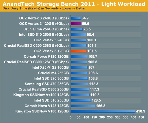
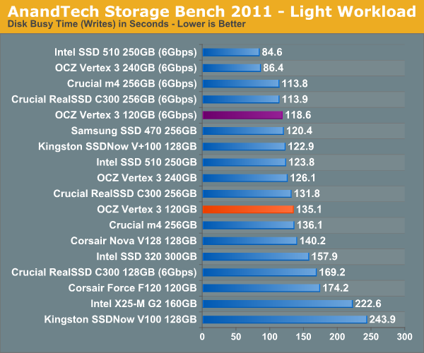
by Anand Lal Shimpi on April 6, 2011 6:32 PM ESTAnandTech Storage Bench 2011 - Light Workload
Our new light workload actually has more write operations than read operations. The split is as follows: 372,630 reads and 459,709 writes. The relatively close read/write ratio does better mimic a typical light workload (although even lighter workloads would be far more read centric).
The I/O breakdown is similar to the heavy workload at small IOs, however you'll notice that there are far fewer large IO transfers:
| AnandTech Storage Bench 2011 - Light Workload IO Breakdown | ||||
| IO Size | % of Total | |||
| 4KB | 27% | |||
| 16KB | 8% | |||
| 32KB | 6% | |||
| 64KB | 5% | |||
Despite the reduction in large IOs, over 60% of all operations are perfectly sequential. Average queue depth is a lighter 2.2029 IOs.
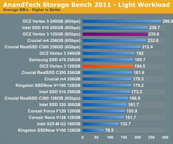
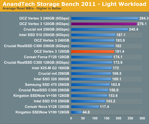
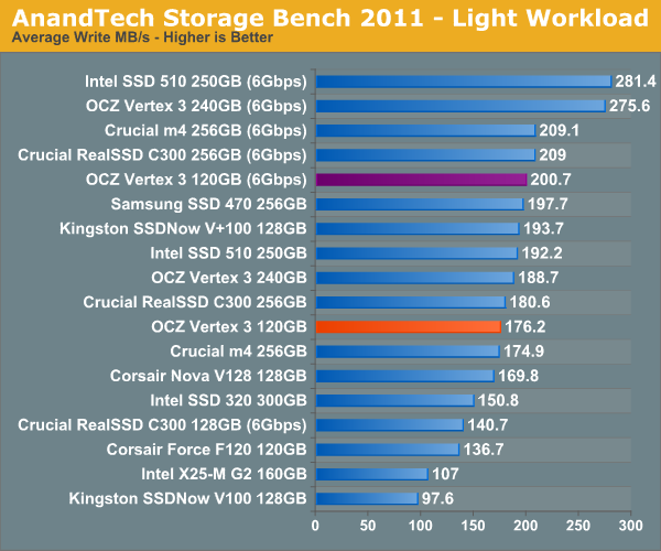
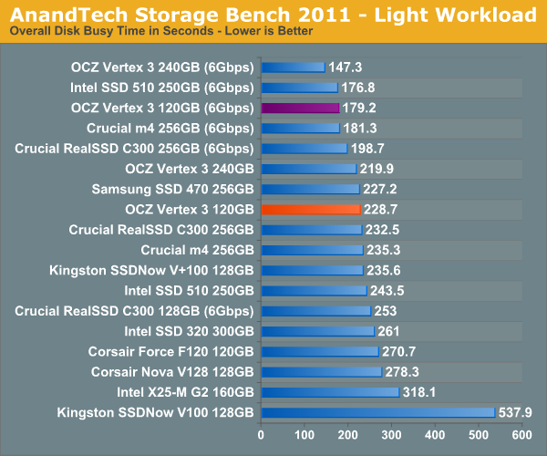
While our heavy 2011 workload may be a little heavy on the writes, the light workload is a bit more balanced. As a result we see the 120GB Vertex 3 move up in the charts a bit more. It's still not as quick as the 240GB drive but it's pretty much quicker than anything else.


153 Comments
View All Comments
dagamer34 - Wednesday, April 6, 2011 - link
Any idea when these are going to ship out into the wild? I've got a 120GB Vertex 2 in my 2011 MacBook Pro that I'd love to stick into my Windows 7 HTPC so it's more responsive.Ethaniel - Wednesday, April 6, 2011 - link
I just love how Anand puts OCZ on the grill here. It seems they'll just have to step it up. I was expecting some huge numbers coming from the Vertex 3. So far, meh.softdrinkviking - Wednesday, April 6, 2011 - link
"OCZ insists that there's no difference between the Spectek stuff and standard Micron 25nm NAND"Except for the fact that Spectek is 34nm I am assuming?
There surely must be some significant difference in performance between 25 and 34, right?
softdrinkviking - Wednesday, April 6, 2011 - link
sorry, i think that wasn't clear.what i mean is that it seems like you are saying the difference in process nodes is purely related to capacity, but isn't there some performance advantage to going lower as well?
softdrinkviking - Wednesday, April 6, 2011 - link
okay. forget it. i looked back through and found the part where you write about the 25nm being slower.that's weird and backwards. i wonder why it gets slower as it get smaller, when cpus are supposedly going to get faster as the process gets smaller?
are their any semiconductor engineers reading this article who know?
are the fabs making some obvious choice which trades in performance at a reduced node for cost benefits, in an attempt to increase die capacities and lower end-user costs?
lunan - Thursday, April 7, 2011 - link
i think because the chip get larger but IO interface to the controller remain the same (the inner raid). instead of addressing 4GB of NAND, now one block may consists of 8GB or 16GB NAND.in case of 8 interface,
4x8GB =32GB NAND but 8x8GB=64GB NAND, 8x16GB=128GB NAND
the smaller the shrink is, the bigger the nand, but i think they still have 8 IO interface to the controller, hence the time takes also increased with every shrinkage.
CPU or GPU is quite different because they implement different IO controller. the base architecture actually changes to accommodate process shrink.
they should change the base architecture with every NAND if they wish to archive the same speed throughput, or add a second controller....
I think....i may not be right >_<
lunan - Thursday, April 7, 2011 - link
for example the vertex 3 have 8GB NAND with 16(8 front and 8 back) connection to the controller. now imagine if the NAND is 16GB or 32 GB and the interface is only 16 with 1 controller?maybe the CPU approach can be done to this problem. if you wish to duplicate performace and storage, you do dual core (which is 1 cpu core beside the other)....
again...maybe....
softdrinkviking - Friday, April 8, 2011 - link
thanks for your reply. when i read it, i didn't realize that those figures were referring to the capacity of the die.as soon as i re-read it, i also had the same reaction about redesigning the controller, it seems the obvious thing to do,
so i can't believe that the controller manufacturer's haven't thought of it.
there must be something holding them back, probably $$.
the major SSD players all appear to be trying to pull down the costs of drives to encourage widespread adoption.
perhaps this is being done at the expense of obvious performance increases?
Ammaross - Thursday, April 7, 2011 - link
I think if you re-reread (yes, twice), you'll note that with the die shrink, the block size was upped from 4K to 8K. This is twice the space to be programmed or erased per write. This is where the speed performance disappears, regardless of the number of dies in the drive.Anand Lal Shimpi - Wednesday, April 6, 2011 - link
Sorry I meant Micron 34nm NAND. Corrected :)Take care,
Anand