LG Optimus 2X & NVIDIA Tegra 2 Review: The First Dual-Core Smartphone
by Brian Klug & Anand Lal Shimpi on February 7, 2011 3:53 AM EST- Posted in
- Smartphones
- Tegra 2
- LG
- Optimus 2X
- Mobile
- NVIDIA
NVIDIA's Tegra 2
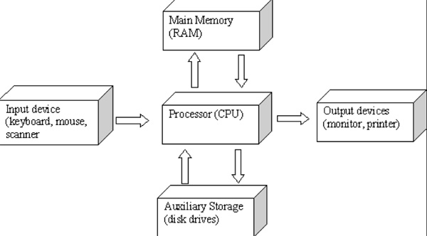
The old definition of a computer is a microprocessor, memory, storage, input and output. The modern definition expands it a bit to include coprocessors (e.g. GPUs) as well as multiple types and levels of memory and storage. The type of input and output devices have changed as well. In smartphones keyboards are virtual and output is integrated into the phone. Although the definition of a computer has evolved, it’s not all that different.
In the old days, almost each one of these parts of a computer was a discrete component. You had a CPU, memory, a hard drive, a video processor (before they were GPUs) all independent of one another. Go back prior to the 486 and you’ll even find that your CPU had to rely on an external FPU for all floating point math.
Moore’s Law has given us bigger, faster, better in all of these areas. Intel’s 486 was the first million transistor x86 processor, introduced in 1989. Sandy Bridge, introduced in January, is just shy of a billion transistors. Sixteen megabytes of memory was a big deal 20 years ago, today high end PCs ship with several gigabytes of memory. Another side effect of Moore’s Law however is integration.
At first integration brought things like the FPU and a second level cache onto the processor die. Over time more components were brought in to the fold. AMD integrated the memory controller in its Athlon 64 processor. Intel brought graphics on-package with Clarkdale/Arrandale, and later on-die with Sandy Bridge. AMD is doing the same with Fusion.
In the smartphone space, the integration is even more pronounced. With physical space and power as major constraints, smartphone chip makers have been forced to further trade performance for integration. The level of integration is so high within a smartphone that you almost never hear about what CPU a phone uses, but rather what Application Processor it uses otherwise known as an SoC (System on Chip or System on a Chip).
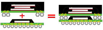
Package on Package (DRAM on top, SoC on bottom)—source: statschippack.com
Integrate a CPU, GPU, memory controller, video decoder, audio decoder, video encoder (sometimes), camera processor, system memory and maybe even a modem onto a single chip and you’ve got something that can only be described as a System on a Chip. It’s a single physical chip that integrates nearly all of the functions of the entire computer. Nearly all of the aforementioned components are on a single piece of silicon, with the exception of any integrated memory. To save board real estate and enable smaller form factors, it’s not uncommon to stack DRAM on top of the SoC package instead of beside it. The SoC in a PoP (Package on Package) stack has contacts on its top surface that line up with the balls on the DRAM for power and signaling. PoP stacks work because the SoC underneath doesn’t dissipate much heat and thus doesn’t mind being insulated by some DRAM up top.
Examples of SoCs are Qualcomm’s Snapdragon, Texas Instruments’ OMAP 4 and of course the subject at hand, NVIDIA’s Tegra 2. Although this is a review of LG’s Optimus 2X, it’s just as much a review of NVIDIA’s Tegra 2.
Tegra 2: The SoC
As a System on a Chip, NVIDIA’s Tegra 2 has a number of processors that make up the whole. Having its roots in the PC industry and being used to briefing inquisitive press, NVIDIA put together this handy die shot that shows the various parts of the Tegra 2:
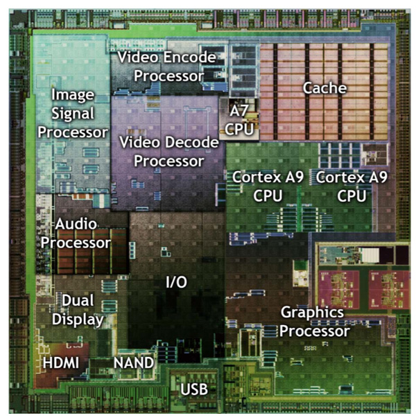
With the exception of two blocks, the Tegra 2 die is entirely NVIDIA’s own creation. The A7 and Cortex A9 blocks are IP licensed from ARM. The entire die is manufactured at TSMC on a 40nm process, similar to NVIDIA’s high end GPUs. While its GPUs are built on TSMC’s 40nm “G” process, Tegra 2 is a slightly different beast.
Most foundries offer two variants of the same manufacturing process: general purpose (G) and low power (LP). The feature size is the same, however the transistors are tuned differently. TSMC’s general purpose process transistors are very fast and low voltage, unfortunately they have very high leakage current. Transistors, as you may know, are electrical on/off switches. Apply a voltage to them and current flows, remove the voltage and current stops flowing. In reality sometimes current flows when you don’t want it to, and this is referred to as leakage. High leakage is a side effect of the nice high performance transistors we need to run the fastest processors.
TSMC’s 40nm LP process uses lower voltage, slower switching transistors (can’t run at as high of a clock speed) that, as a result, have very low leakage characteristics. The lower your leakage and the lower your voltage, the lower your overall power is.
For an SoC, you’d assume that the whole thing would be built at the 40nm LP process. See those two Cortex A9 cores in the diagram above? Remember how they’re licensed from ARM? Those things are pretty high performance, they run at 1GHz. Everything else in the chip runs at 300MHz or less for the most part. On top of that, the libraries ARM provides are optimized for TSMC’s 40nm G process.
As a result, Tegra 2 uses a mixture of G and LP 40nm transistors on two separate voltage rails. The two Cortex A9 cores and the L2 cache are built using TSMC’s 40nm G process transistors, while the rest of the SoC (including the GPU) is built using 40nm LP transistors. The pair of A9s can be powered down together although not independently. We’ll get to a deeper discussion of the ARM Cortex A9 shortly.
The ISP (Image Signal Processor), located in the upper left of the die shot above, is responsible for taking the output from a camera (still/video) controller and processing into a usable video state. The Tegra 2 ISP is capable of processing images at a rate of 80 megapixels per second. The ISP supports two cameras, a 12 megapixel primary and a 5 megapixel secondary. The math works out to a maximum of 6 frames per second captured from the primary sensor at 12MP. LG uses the Tegra 2’s ISP to enable a 6 fps burst mode as you’ll see later on in the review, unfortunately it only works at a 2MP resolution. NVIDIA’s strong ISP looks better on paper than in practice it seems.
The video encode processor does real time H.264 video encoding, which is used when capturing video from the camera sensor. NVIDIA doesn’t provide any specs on what the encoder is capable of, but we’re not too impressed with the quality of its output (again, you’ll see more later).
The audio processor is dedicated hardware for audio encoding and decoding. This is used for audio capture as well as audio playback. Even MP3 playback is done on the dedicated audio processor so the Cortex A9s remain powered down to maximize battery life.
The Tegra 2 video decoder can fully accelerate the decode of 1080p H.264 Baseline profile videos at up to 20Mbps. The specs mostly look good on paper as you won’t be playing anything near that bitrate on your smartphone. NVIDIA includes dual-display capabilities with Tegra 2. The SoC can output the frame buffer to the smartphone’s display as well as an external display via HDMI out.
The ARM A7 nestled in between the video decoder and the L2 cache is used as a system management core. It handles communication between blocks, power management and general SoC management. The remaining blocks (outside of I/O) are the two CPU cores and the GPU. Those both require a lot more detail.


75 Comments
View All Comments
rpmrush - Monday, February 7, 2011 - link
Solid review, but please at least use spell check. I'm not a grammar or typo freak, but there were way too many simple typos that spell check wouldn't even let you get by with. At least have someone proof read it before you publish to the public.zowie - Tuesday, February 8, 2011 - link
who can create a new type battery, who will be the richest man in the worlduhuznaa - Tuesday, February 8, 2011 - link
Yeah, and until then those who manage to come up with some decent power management will be the richest...Seriously, every improvement on the battery front almost always just leads to devices drawing more power. It's somewhat ironic that last year's iPhone still leads the pack when it comes to battery life. Power management (that is: don't draw more power than absolutely necessary by throttling or shutting down components that aren't needed or aren't fully needed in a given moment) is hard and boring design work nobody seems to care for. And with devices and software getting replaced with the next iteration every few months this is even understandable, it's just not worth the effort, especially when nobody seems to care and benchmarks are so much more important to the crowd.
DanNeely - Tuesday, February 8, 2011 - link
How is is typically played back: Cropped, or vertically resampled?Wilco1 - Tuesday, February 8, 2011 - link
Tegra 3 has 4 1.5GHz Cortex-A9's according to a leaked slide.That was a great article! A few minor corrections: The ARM11 VFP is fully pipelined (so it can beat the A8 on FP performance). Like the A8, Scorpion is 2-way in-order, not limited out-of-order. In-order cores issue instructions in-order but may complete them out-of-order. On the other hand, OoO cores use register renaming to issue instructions out-of-order but complete them in-order.
Note none of the micro benchmarks used emits Neon instructions. JIT compilers don't have enough time to generate high quality code, let alone autovectorize! For proper benchmarking you will need to run native code compiled with a quality compiler (not GCC - it is still far behind the state of the art on ARM, especially Thumb-2).
metafor - Tuesday, February 8, 2011 - link
I would argue with that definition of OoO. A design does not need register renaming in order to issue any arbitrary instruction OoO. It's simply a trade-off of whether to centralize hazard tracking on register accesses or on retirement.PWRuser - Tuesday, February 8, 2011 - link
Excellent review. Please, in your future reviews don't stop including gems like this one:"Generally while browsing I can feel when Flash ads are really slowing a page down - the 2X almost never felt that way."
That's what matters! Including hands on observations along with a full volley of synthetic benchmarks.
This review comes as close as humanly possible to portraying a handset's ability to readers without the said readers trying it out.
Your attention to detail puts other reviews to shame. Keep up the good work.
sarge78 - Tuesday, February 8, 2011 - link
Don't forget about ST-Ericsson's U8500 A9. They could be a major player in 2011/2012 with potential design wins from Nokia and Sony Ericsson.warisz00r - Tuesday, February 8, 2011 - link
What equipments do you use to test the phone's audio quality with?phut- - Tuesday, February 8, 2011 - link
"NVIDIA tells us that the Tegra 2 SoC is fully capable of a faster capture rate for stills and that LG simply chose 2MP as its burst mode resolution. For comparison, other phones with burst modes capture at either 1 MP or VGA. That said, unfortunately for NVIDIA, a significant technological advantage is almost meaningless if no one takes advantage of it. It'll be interesting to see if the other Tegra 2 phones coming will enable full resolution burst capture. unfortunately for NVIDIA, a significant technological advantage is almost meaningless if no one takes advantage of it. It'll be interesting to see if the other Tegra 2 phones coming will enable full resolution burst capture. meaningless if no one takes advantage of it. It'll be interesting to see if the other Tegra 2 phones coming will enable full resolution burst capture."LG have probably made this decision based on the sensitivity of the invariably minuscule sensor they will have used. Having 6 frames of 12mp is pointless if they are 12 incomprehensible megapixels due to the lacklustre sensitivity of the pixels in their chosen part.
The kind of sensor you find delivering a meaningful burst in something like a 5D mk2 is enormous and power hungry, in comparison to an operating environment such as a phone.