Intel's Sandy Bridge Architecture Exposed
by Anand Lal Shimpi on September 14, 2010 4:10 AM EST- Posted in
- CPUs
- Intel
- Sandy Bridge
Final Words
Intel is trying out a new approach to sharing information about its technologies. In an attempt to surprise the market (and potentially positively impact stock price), Intel is keeping details on upcoming products quiet until it gets closer to launch. This is why we didn’t hear about Sandy Bridge until after we were able to preview its performance a couple of weeks ago. I can’t say I’m a fan of the new approach, but it does make things a little more exciting.
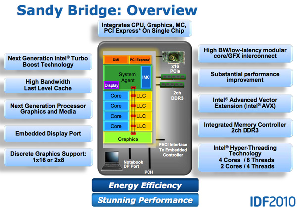
And exciting Sandy Bridge is. The CPU architecture itself doesn’t look too revolutionary. These are the sorts of improvements we’ve come to expect from Intel from one generation to the next. The out of order execution window grew as did all associated buffers. Thanks to some significant redesigns in hardware Intel was able to increase branch prediction accuracy and FP execution throughput all while making the chip more energy efficient.
Improved turbo will surely be appreciated. More aggressive turbo bins plus the ability to turbo up above TDP limits for short periods of time will help make PCs feel more responsive even when doing relatively benign tasks. Things like launching applications, loading web pages or just opening new window stand to benefit.
The architecture sounds a lot like Intel simply did Nehalem/Westmere better. Over time you come up with newer, better ways to do things and that’s ultimately what Sandy Bridge looks like - a better, more efficient way to do what Conroe, Nehalem and Westmere did before it.
The more dramatic changes happened outside of the cores. GPU performance is clearly an important Sandy Bridge feature as we’ve already shown. I can’t help but be curious about how far Intel could take its SNB graphics subsystem if it simply scaled up the number of EUs. The media processing engine, particularly with the video transcode support is very exciting. Assuming image quality is maintained and there’s good software support at launch, this could very well be Sandy Bridge’s killer feature. The ability to transcode at over 10x real time on everything from a desktop to a notebook is just awesome. With good software support, SNB’s video transcode engine could effectively stop consumer GPU based video encoding in its tracks. The improved video decode engine is also a welcome addition to the Sandy Bridge architecture.
Connecting it all together we have Sandy Bridge’s ring bus. Generally microprocessor designs don’t undergo such a radical changes unless the design will be used for a while to come. The ring bus sounds very scalable and should support growth in core count, L3 cache and GPU performance. This may end up being the base architecture that takes us from multi-core to many core.
Mobile Sandy Bridge is significantly faster than Arrandale/Clarksfield
Sandy Bridge will ship in Q1 2011 for both notebooks and desktops and from what we’ve heard, pricing will be very compelling. If you're interested in a sneak peak of Sandy Bridge's performance, take a look at our preview here.


62 Comments
View All Comments
name99 - Tuesday, September 14, 2010 - link
This is no secret. This is exactly Intel's tick-tock strategy that has been in place for years now.The one thing you have to keep in mind is that designing these CPUs now takes of order SEVEN YEARS (!!!) from conception to ship, which means that slips and mistakes do occur. Intel (and I guess AMD) have to make their best guess as to what the market will look like in seven years and sometimes they do guess incorrectly. Of course there is scope for small changes along the way closer to the release date, but not for changes in the grand strategy.
medi01 - Tuesday, September 14, 2010 - link
Agreed, it was two things: greed and the fact that AMD is currently not in a position to be a threat.tatertot - Tuesday, September 14, 2010 - link
"The value segments won’t see Sandy Bridge until 2012."You later show a roadmap slide which indicates Sandy Bridge in the value segment in Q3 2011.
Perhaps you meant "H2 '11" instead of "2012" ?
J_Tarasovic - Thursday, September 16, 2010 - link
I think that the roadmap probably refers to OEM shipments, whereas, Anand was probably referring to when consumers would actually be able to buy devices.iwodo - Tuesday, September 14, 2010 - link
I just realize that my computer will no longer scream when i do WebCam Video Conferencing with Skype!. With the Encoder Engine and Decoder Engine, all i am doing it feeding USB 3.0 data and move them around........yuhong - Tuesday, September 14, 2010 - link
"Back in the Core Duo days that was 80-bits of data. When Intel implemented SSE, the burden grew to 128-bits. ""Core Duo" Huh?
NaN42 - Tuesday, September 14, 2010 - link
No, it seems to be right. Core Duo belongs to the Pentium M microarchitecture which implemented the SSE registers as two 64bit registers. So the largest registers were the x87-registers, but I'm not sure whether upon register renaming the registers were really copied.aka_Warlock - Tuesday, September 14, 2010 - link
New CPU from Intel... and guess what?!! New SOCKET!! Lol.Intel do know how to milk the stupid cow.
bernpi - Sunday, November 14, 2010 - link
For most people it makes perfect sense to get a new socket. Most people don't buy every new CPU from Intel or AMD because it would be a waste of money. My current CPU is a Core2Duo Quad processor with a 775 socket, i skipped the nehalem generation and will buy a SandyBridge early next year. So why should i keep my motherboard and the old 775 socket? Of course i will buy a new motherboard for the new processor. So i think for most people this is not a real issue.Sahrin - Tuesday, September 14, 2010 - link
There's a lot of "neato" stuff that does a lot to improve the user experience by making the chip use its design resources more intelligently (smarter turbo - that 'comcast turbo-boost' feature should really make a difference for end users); but in terms of actual throughput it looks like Intel left FP performance the same; and there certainly isn't any new integer hardware.K11, on the other hand, doubled integer ALU's (though the raw number of execution units is now the same as in a Nehalem core) and added a half-width (compared to Intel) FP unit.
First, I'd be interested to see if the whizz-bangies AMD was talking about for the K11 FPU a year ago make the execution time for 128-bit FP instructions comparable, better than, or still slower than Intel's FPU .
Second, I'd be quadruple interested to see what impact the way AMD is allocating the new integer hardware is going to have on performance. A monolithic Nehalem core is going to be able to handle more complex (wider) threads better than a K11 core (that's a 2-integer and 1-FPU Bulldozer); but in SMT-mode (or pseudo-SMT mode) what happens? We know Intel experiences a performance hit in HTT mode which they are only able to offset because Nehalem is so wide. AMD thinks it isn't going to get the expected hit in the front end, and they won't have the thread-switching penalty that Intel does. My prediction is that 8-core K11/Bullzoder will crush Sandy Bridge in multithreaded FP-light workloads and be 5-20% slower in everything else (the possible exception being 128-bit floats).
I'm actually kind of disappointed by this update to Nehalem...Intel did a lot of "uncore" stuff and implemenated AVX. Where's our wider back-end? More execution hardware drives better single-thread performance...the rest is just undoing the damage from the CISC-RISC transition in the front end and OoO .