Intel's Sandy Bridge Architecture Exposed
by Anand Lal Shimpi on September 14, 2010 4:10 AM EST- Posted in
- CPUs
- Intel
- Sandy Bridge
The Ring Bus
With Nehalem/Westmere all cores, whether dual, quad or six of them, had their own private path to the last level (L3) cache. That’s roughly 1000 wires per core. The problem with this approach is that it doesn’t work well as you scale up in things that need access to the L3 cache.
Sandy Bridge adds a GPU and video transcoding engine on-die that share the L3 cache. Rather than laying out another 2000 wires to the L3 cache Intel introduced a ring bus.
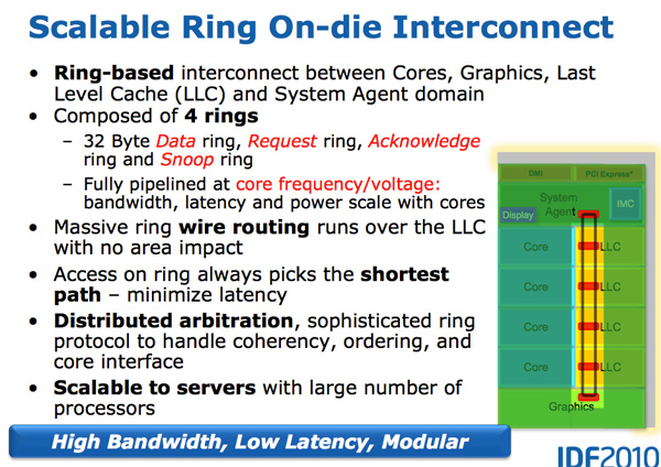
Architecturally, this is the same ring bus used in Nehalem EX and Westmere EX. Each core, each slice of L3 (LLC) cache, the on-die GPU, media engine and the system agent (fancy word for North Bridge) all have a stop on the ring bus.
The bus is made up of four independent rings: a data ring, request ring, acknowledge ring and snoop ring. Each stop for each ring can accept 32-bytes of data per clock. As you increase core count and cache size, your cache bandwidth increases accordingly.
Per core you get the same amount of L3 cache bandwidth as in high end Westmere parts - 96GB/s. Aggregate bandwidth is 4x that in a quad-core system since you get a ring stop per core (384GB/s).
L3 latency is significantly reduced from around 36 cycles in Westmere to 26 - 31 cycles in Sandy Bridge. We saw this in our Sandy Bridge preview and now have absolute numbers in hand. The variable cache latency has to do with what core is accessing what slice of cache.
Also unlike Westmere, the L3 cache now runs at the core clock speed - the concept of the un-core still exists but Intel calls it the “system agent” instead and it no longer includes the L3 cache.
With the L3 cache running at the core clock you get the benefit of a much faster cache. The downside is the L3 underclocks itself in tandem with the processor cores. If the GPU needs the L3 while the CPUs are downclocked, the L3 cache won’t be running as fast as it could had it been independent.
The L3 cache is divided into slices, one associated with each core although each core can address the entire cache. Each slice gets its own stop and each slice has a full cache pipeline. In Westmere there was a single cache pipeline and queue that all cores forwarded requests to, in Sandy Bridge it’s distributed per cache slice.
The ring wire routing runs entirely over the L3 cache with no die area impact. This is particularly important as you effectively get more cache bandwidth without any increase in die area. It also allows Intel to scale the core count and cache size without incurring additional ring-related die area.
Each of the consumers/producers on the ring get their own stop. The ring always takes the shortest path. Bus arbitration is distributed on the ring, each stop knows if there’s an empty slot on the ring one clock before.
The System Agent
For some reason Intel stopped using the term un-core, instead in Sandy Bridge it’s called the System Agent.
The System Agent houses the traditional North Bridge. You get a 16 PCIe 2.0 lanes that can be split into two x8s. There’s a redesigned dual-channel DDR3 memory controller that finally restores memory latency to around Lynnfield levels (Clarkdale moved the memory controller off the CPU die and onto the GPU).
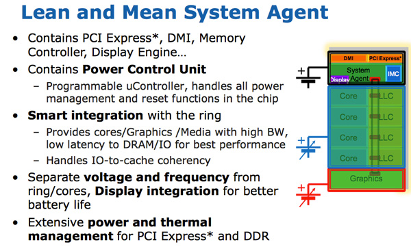
The SA also has the DMI interface, display engine and the PCU (Power Control Unit). The SA clock speed is lower than the rest of the core and it is on its own power plane.


62 Comments
View All Comments
yuhong - Tuesday, September 14, 2010 - link
There is no VEX.256 for 256-bit integer ops, but there is a VEX.128 prefix that zeros the upper part of YMM registers to reduce the delays..NaN42 - Tuesday, September 14, 2010 - link
Well, I found a summary of the prefixes. Interestingly there are some exception, like I guessed, e.g. a VEX.128 prefix does not exist for conversion of packed floating points<->packed integers and for CRC32c + POPCNT.CSMR - Tuesday, September 14, 2010 - link
Anand:The best info available on an exciting platform, good job.
I wonder if for the next article you could test DirectX / OpenGL compatibility? Intel advertises compliance for a lot of its products, but in reality the support is partial, and some applications that use DirectX / OpenGL entirely correctly are not supported by Intel graphics, including the current HD graphics.
I've found this with fastpictureviewer (DirectX, I think 9) and Photoshop CS5 (OpenGL 2)
This is quite shocking. Given that Intel is doing this currently, it would be great if reviewers could prod it into action, but unfortunately they tend to place speed first, correctness second or nowhere.
marass31 - Thursday, September 16, 2010 - link
Hi CSMR,Could you please write more details about problems with DX and OGL on Intel HD graphics( including gfx driver version, system config ...). You mentioned about two applications: Fastpictureviewer and PSCS5, so could you please write some steps to reproduce to each of them - THX a lot.
ssj4Gogeta - Tuesday, September 14, 2010 - link
What's the point of extreme editions if we're going to have affordable K SKUs?Or will socket 2011 not have any K SKUs? I'm guessing they'll leave the BCLCK unlocked on the 2011, and only have normal and extreme processors (no K processors). Or maybe extreme editions will just have more cores like 980X?
DanNeely - Tuesday, September 14, 2010 - link
The extreme editions have always been for people who buy retail or who're playing with LN2 and need the most insanely binned part available. They've never been a mainstream OCer part.MonkeyPaw - Tuesday, September 14, 2010 - link
I have a bad feeling about the "k" chips and the future of overclocking. Sure, intel gave us turbo mode, but that almost seems like appeasement before the last shoe drops. First, limited turbo with good overclockng, then better turbo and less overclocking, and now it's sounding like slightly better turbo and even less overclocking. It looks like we are moving to intel-controlled overclocking. There's virtually no value left for the enthusiast--a user that is already just a small part of the market. Intel just decided what the enthusiast needs, but I don't think they get what those users actually want.I just don't buy that these limits are to prevent fraud. Mom and Pop stores are virtually all gone now, and I'd hate to think what Intel would do to a Dell or HP if they got caught overclocking desktops.
I guess this leaves another door open for AMD. Sad, cause SnB looks like a great design.
This Guy - Wednesday, September 15, 2010 - link
Hopefully Intel will allow the 'energy budget' to be increased when an extreme edition processer detects less thermal resistance (i.e. a bloody big heat sink). This would allow an EE CPU to either run with a higher multiplier or run at it's turbo frequency longer. (I'ld like this feature on all CPU's)This would make EE CPU's interesting if K CPU's catch up in terms of cores.
Shadowmaster625 - Tuesday, September 14, 2010 - link
What are the prospects for using Intel's transcoder to convert DVDs to 700MB avi files? Either DivX, Xvid, or H.264? Or anything else better than MPEG-2?Dfere - Tuesday, September 14, 2010 - link
Since this seems to be, overall, a refinement, and not so much an improvement with new capabilities, and Anand's comments about the scalability of GPU related enhancements, that Intel is taking a two step approach towards CPU releases, in addition to its fab strategies? E.G, we see a new CPU, then it gets shrunk, then it gets improved (like this), then it gets bells and whistles (like a GPU etc), then we start over again with a really new architecture.....