Everything You Always Wanted to Know About SDRAM (Memory): But Were Afraid to Ask
by Rajinder Gill on August 15, 2010 10:59 PM ESTEvery read/write memory transaction can be segmented by type into one of three performance bins depending on the status of the bank/page to be accessed. These bins, in order of best to worst, are page-hit, page-empty, and page-miss. For the most part, anything we can do to increase the number of page-hit transactions or reduce the number of page-miss transactions is a good thing.
A page-hit access is defined as any read or write operation to an open page. That is, the bank containing the open page is already active and is immediately ready to service requests. Because the target page is already open, the nominal access latency for any memory transaction falling into this category is approximately tCAS (the CAS Latency of the device).
Click to enlarge
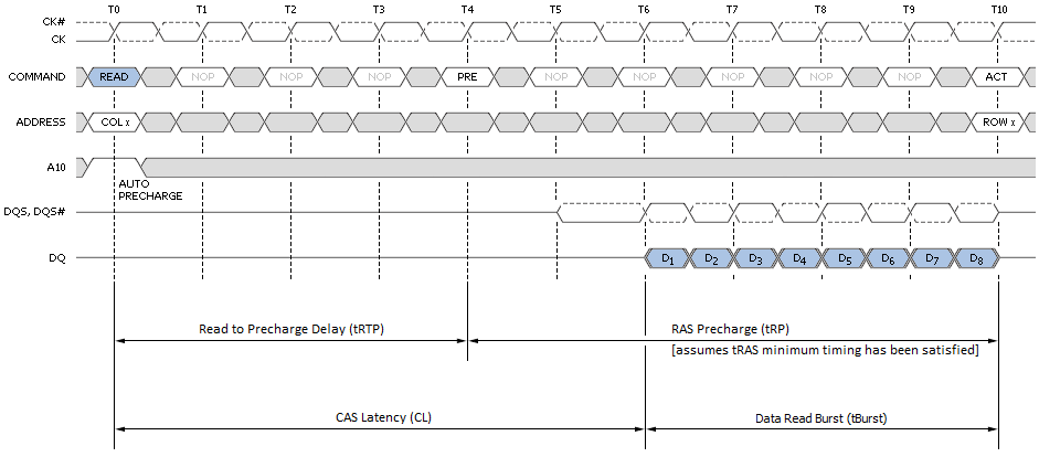
Figure 6 shows the minimum read latency associated with a best-case page-hit scenario. For a part with a CAS Latency of 6T, the memory controller waits only six short clocks before the start of data return. During a Read with Auto-Precharge, the Read command will execute as normal except the active bank will begin precharging CAS-latency (CL) clock cycles before the end of the burst. This feature allows the precharge operation to be partially or completely hidden during periods of burst read cycles, dependent on CL. When tuning our systems we always seek to set tRTP such that tRTP + tRP equals CL + tBurst for exactly this reason. Put another way, if CL and tRP are the same set 4T for DDR3 (2T for DD2).
Sequential reads to the same page make these types of transactions even more profitable as each successive access can be scheduled at a minimum of tBurst (4T) clocks from the last. The timing is captured as the CAS-to-CAS Delay (tCCD) and is commonly referred to as 'Back-to-Back CAS Delay' (B2B), as shown per Figure 7. This feature makes possible extremely high data transfer rates for total burst lengths of one page or less - in our case, 8KB.

Click to enlarge
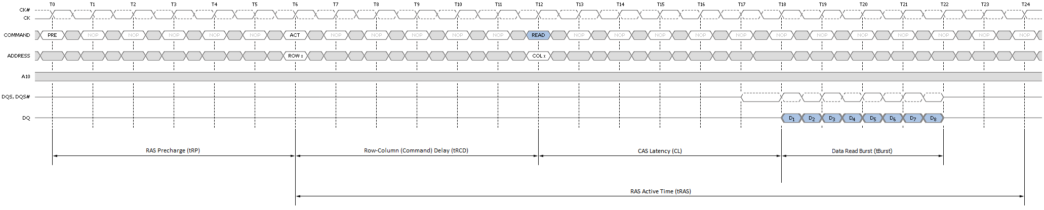
Although not ideal, a page-empty access is still preferred to a miss. In this case the bank to be accessed is Idle with no page open. Common sense tells us any attempt to read or write data to a page in this bank first requires we Activate the bank. In other words, nominal access latency now includes the time to open the page - Row-Column (or Command) Delay (tRCD). This is a doubling of the minimum access latency when compared to that of the page-hit case! Twelve cycles (tRCD + CL) now elapse before the first word is returned. Figure 8 shows this the detail.
![]()
Click to enlarge
Finally, as if the relative penalty of page-empty access wasn't bad enough, here comes page-miss. A miss occurs anytime a memory transaction must first close an open page in order to open an alternate page in the same bank. Only then can the specified data access take place. First closing an open page requires a Precharge, adding the RAS Precharge (tRP) delay to any already lengthy operation. As you can see by Figure 9, the nominal latency of an access of this type is three times that of one page-hit operation!
Click to enlarge
The relative gain/loss ratio for each access type can be quickly assessed simply through a cursory review of the most basic device timings. Imagine a memory kit rated for operation at DDR3-1600, 6-6-6-18 (CL-tRCD-tRP-tRAS): With nothing more we can estimate six cycles for a page-hit access, 12 cycles for a page-empty access, and 18 cycles for a page-miss access.
Normalized to the page-hit access latency, page-empty access is twice as long, and page-miss access is a whole three times as long. If we combine this with what we know about the inner functions of the SDRAM state machine we see page-hit and page-miss are really just subsets of the same bank state (active). Of course, page-empty access necessarily implies an idle bank. The following proof rewards us with some powerful insight.
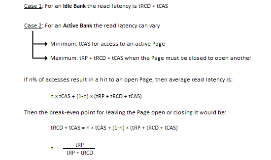
The variable n also represents the percentage of accesses to banks with open pages that must result in a page-hit access if we are to simply pace the nominal access latency that would be achieved if every read access was to an idle bank. And the only thing this depends on is the RAS Precharge delay and the Row-Column (or Command) Delay of the device in question.
You would think by working to maximize n, performance would be maximized as well. And you'd be right. Let's take what we've learned thus far and step it up a notch. We promise, after this you'll never see memory timings in the same light ever again.
Before proceeding, we've prepared a video for those of you that would like to view a few simple animations meant to help visualize each transaction type:


46 Comments
View All Comments
mupilot - Monday, August 16, 2010 - link
Nice article, its very in depth, but easy to read! I'll have to read through a couple times if I truly want to understand how my memory works so I can actually understand what I'm doing when I overclock my memory and adjust the timings.Cool Mike - Monday, August 16, 2010 - link
I find memory a bit confusing. What type of memory would be best (or even work) on an AMD system - for example the Asus M4N98TD EVO. Will the lower voltage modules work? I'd like to get some pretty decent memory, but almost all of the discussions are around Intel based chipsets. Any help would be appreciated.vajm1234 - Monday, August 16, 2010 - link
---- well i too wanna see a comparison how AMD works against the intelPrinceGaz - Monday, August 16, 2010 - link
Whilst the text for the Mistake Counter is incorrect, the bit count in the table does match the text-- the PARAMS2 register holds the 9, not 8 MSBs of each parameter (the internal values being 13 bit, not 12 bit), and the text and diagram both agree on this.PrinceGaz - Monday, August 16, 2010 - link
Oh and by the way, thankyou for an extremely informative article which has refreshed (hehe) and added to what I knew about how RAM operates and the effects of the main timings.Icepop66 - Monday, August 16, 2010 - link
Thanks for touching on some of the important aspects of sdram architecture and function and how they're related. My understanding is better now. Thanks for consistently good articles and reviews.Gary Key - Monday, August 16, 2010 - link
Rampage III Extreme -BIOS 0878 -
1. Opened Memory Timing Selections for Ultimate Tweaking
2. General Performance Enhancements for Overclocking
3. AnandTech Memory Article BIOS - Support provided by ASUS USA Tech Support (that would be me).
http://www.mediafire.com/?850dsymmc9j7jdd
lowenz - Monday, August 16, 2010 - link
Simply AWESOME article!Muhammed - Monday, August 16, 2010 - link
You didn't mention the fact that (for example) DDR3 1600MHz actually works @200 MHz , and by fetching 8-bits per clock , it can effectively work like a 1600MHz RAM .DDR2 @800 MHz , actually works at 200MHz too but fetching 4-bits per clock .
DDR@400 MHz , actually works at 200MHz too , fetching 2-bits per clock .
MrBrownSound - Monday, August 16, 2010 - link
Thank you for helping me understand. Yes I was afraid to ask, or maybe I just felt I didn't need to know. I was wrong.