ASUS Maximus III Extreme - P55 for $349
by Rajinder Gill on April 26, 2010 1:32 AM EST- Posted in
- Motherboards
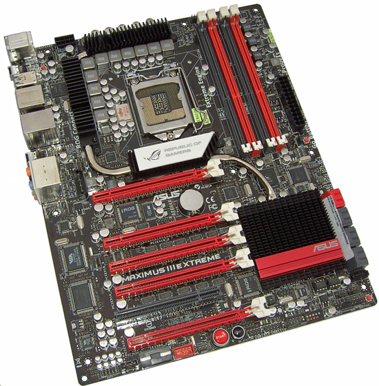
In terms of layout this board is just a ‘souped-up’ Maximus III Formula. Careful inspection of both boards suggest that ASUS have not made any real adjustments other than to add a beefier VRM for the CPU and the addition of SATA 6G, USB 3 and the NF200 bridge chip. The positives are that the M3E should hit the floor running because it’ll use the same basic BIOS backbone of the M3F.
Some might be disappointed to find that the cooling assembly is a single unit – connecting the CPU VRM, NF200 bridge chip and the P55 PCH together with a heatpipe. We found that temps for all three areas are well controlled unless you ramp PWM switching frequency into the 800KHz~1Mz region. In such instances, the assembly does get hot although we did not have any problems with stability as a result. You can use a small latch-on fan to cool the assembly by a few degrees if need be.
The good news is that ASUS have used screw fittings rather than push-pins to attach the heatsink to the board. Although this is a step in the right direction, we’d liked to have seen the use of back plates behind the PWM FET’s to provide a little more rigidity and prevent the central FETs from pulling away when the board bows under pressure from some after-market coolers.
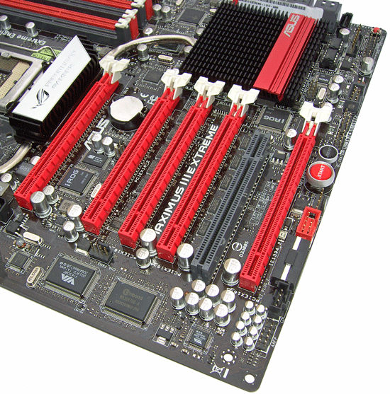
Slot spacing is geared for multi-GPU setups, with lane allocation divided to allow for quad SLI or CrossFire. A couple of Molex connectors are placed on the board to bolster PCIe voltage when all slots are loaded with high performance GPUs that are heavily overclocked.
A single PCI slot is available for older devices, and remains accessible in most configurations should you need to use it.
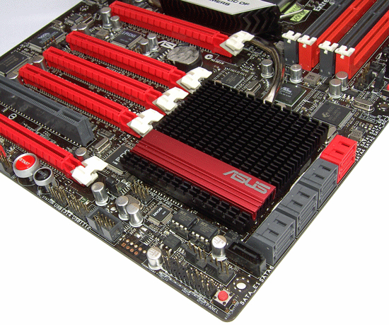
Nine SATA ports are placed in the lower right hand corner of the board, eight are right angled with one placed head on for easy access.
Two BIOS chips are utilized allowing users to flash different BIOS versions for comparison purposes and as a failsafe. Switching between both is done either via BIOS, ROG Connect or by using the red push-button at the lower right corner of the board (LEDs indicate which BIOS is in use).
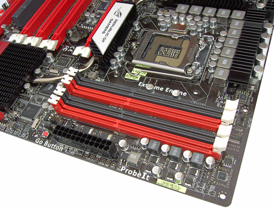
The DIMM slot area is surrounded by voltage measurement pads, ASUS’s GO button (to load saved profiles or to recover the board to safe mode and help it to post) and also an LN2 cooling mode jumper to help the board POST when processors are cooled with liquid nitrogen. We did try the LN2 jumper with our Clarkdale processors to see if they help the board to POST below -110 and found that it was not much help at all. Like other boards out there, we had to mod the 750 ohm PEGR BIAS compensation resistor to a lower value to alleviate cold-boot lock ups at low temperatures.
The onboard measurement points could do with being moved to a location where access is not hampered by cabling. Their current location is not ideal because the ATX 12V cable blocks access somewhat.
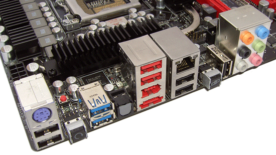
The rear panel I/O set is made up of 1 x PS2, 2 x USB 3.0 ports, 6 x USB ports, 1 x 1394, 1 x Optical S/PDIF, 1 x CMOS clear switch, 1 x ROG Connect switch, 1 x ROG USB port, 1 x RJ45 and six audio I/O connectors.


22 Comments
View All Comments
Nickel020 - Tuesday, April 27, 2010 - link
Thanks for the reply Raja!I think you got me wrong though, I did not mean to say your benchmarking was sloppy, I meant to say that I fully trust your numbers! AT is one of the few sites that I trust to make a sanity check of their benchmark numbers before posting them^^
The numbers did not really make sense to me before because I did not know what you just explained, but now they do make sense, thanks again :)
Rajinder Gill - Tuesday, April 27, 2010 - link
HiNo worries. When I first saw this it had me scratching my head (and other areas of my body). You caught me at a time where I was in an overly self-protective mood (gotta get some sleep)..lol
later
Raja