ASUS Maximus III Extreme - P55 for $349
by Rajinder Gill on April 26, 2010 1:32 AM EST- Posted in
- Motherboards
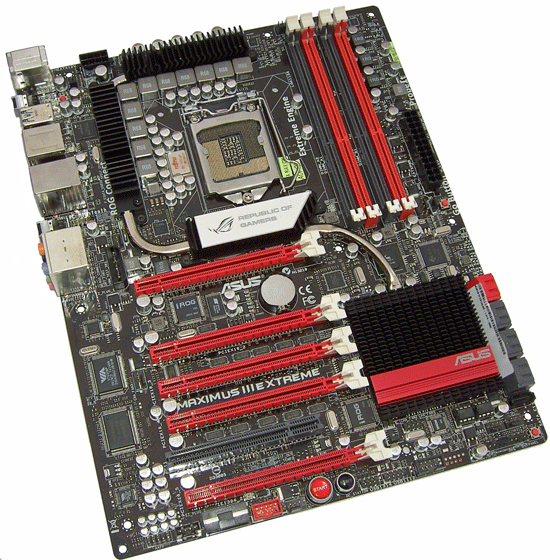
In terms of layout this board is just a ‘souped-up’ Maximus III Formula. Careful inspection of both boards suggest that ASUS have not made any real adjustments other than to add a beefier VRM for the CPU and the addition of SATA 6G, USB 3 and the NF200 bridge chip. The positives are that the M3E should hit the floor running because it’ll use the same basic BIOS backbone of the M3F.
Some might be disappointed to find that the cooling assembly is a single unit – connecting the CPU VRM, NF200 bridge chip and the P55 PCH together with a heatpipe. We found that temps for all three areas are well controlled unless you ramp PWM switching frequency into the 800KHz~1Mz region. In such instances, the assembly does get hot although we did not have any problems with stability as a result. You can use a small latch-on fan to cool the assembly by a few degrees if need be.
The good news is that ASUS have used screw fittings rather than push-pins to attach the heatsink to the board. Although this is a step in the right direction, we’d liked to have seen the use of back plates behind the PWM FET’s to provide a little more rigidity and prevent the central FETs from pulling away when the board bows under pressure from some after-market coolers.
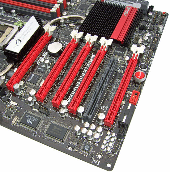
Slot spacing is geared for multi-GPU setups, with lane allocation divided to allow for quad SLI or CrossFire. A couple of Molex connectors are placed on the board to bolster PCIe voltage when all slots are loaded with high performance GPUs that are heavily overclocked.
A single PCI slot is available for older devices, and remains accessible in most configurations should you need to use it.
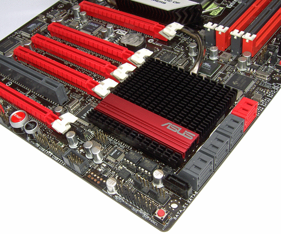
Nine SATA ports are placed in the lower right hand corner of the board, eight are right angled with one placed head on for easy access.
Two BIOS chips are utilized allowing users to flash different BIOS versions for comparison purposes and as a failsafe. Switching between both is done either via BIOS, ROG Connect or by using the red push-button at the lower right corner of the board (LEDs indicate which BIOS is in use).
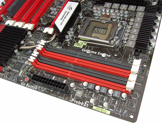
The DIMM slot area is surrounded by voltage measurement pads, ASUS’s GO button (to load saved profiles or to recover the board to safe mode and help it to post) and also an LN2 cooling mode jumper to help the board POST when processors are cooled with liquid nitrogen. We did try the LN2 jumper with our Clarkdale processors to see if they help the board to POST below -110 and found that it was not much help at all. Like other boards out there, we had to mod the 750 ohm PEGR BIAS compensation resistor to a lower value to alleviate cold-boot lock ups at low temperatures.
The onboard measurement points could do with being moved to a location where access is not hampered by cabling. Their current location is not ideal because the ATX 12V cable blocks access somewhat.
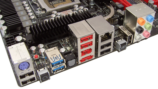
The rear panel I/O set is made up of 1 x PS2, 2 x USB 3.0 ports, 6 x USB ports, 1 x 1394, 1 x Optical S/PDIF, 1 x CMOS clear switch, 1 x ROG Connect switch, 1 x ROG USB port, 1 x RJ45 and six audio I/O connectors.


22 Comments
View All Comments
gasgas - Monday, April 26, 2010 - link
Outstanding review anand, some very nice features on the ASUS board, one has to ask though, if P55 is costing this much is it really worth the effort, why not just get a budget X58 and have more on tap.Makaveli - Monday, April 26, 2010 - link
Why are the screenshots so big?I felt I should have been wearing glasses or something... and I don't wear glasses!
classy - Monday, April 26, 2010 - link
$350 is too much for P55. You can get a serious X58 board for that kind of moneyloghead - Monday, April 26, 2010 - link
good luck to everyonedingetje - Tuesday, April 27, 2010 - link
wouldn't pay more than 100 bucks for it though :)v12v12 - Tuesday, April 27, 2010 - link
I dunno maybe it's me, but we're talking near $400 for a system board? Three-hundred and fifty dollars (& ~$26 tax), that's just lunacy to even bother with. Has anyone ever done some basic, logical mathematics on cost/performance? These so-called "performance/'OC'er" mobos offer barely any noticeable advantages over a solid mid-level board vs the exuberant price people will rationalize. Paying nearly 100% more for hardly 15% performance advantage? For the same money you could buy enhanced cooling equipment for your mid-level board and soar past that waste of a PCB, dollar for dollar.The fanaticism over these "top-end," yet financially inefficient mobos, is just laughable; even the suggestion of purchasing one is also. People are rationalizing spending MORE, for lesser performance per dollar; THIS is ILLOGICAL, and stupid? I say Anand spend more time on solid mid to lower-upper builds vs playing fantasy article on a "gold-sample" OC'er board that offers little in reality for; I dunno maybe ~90% of the readership, whom will not be purchasing boards anywhere near that price range? Articles like these waste the writers' time and the readers'. Also it's money down the drain from a budget, which could be spent on better informing majority of the readers on systems they can actually afford or save for. $349, come on lol. That's a very nice trip somewhere on a plane, buddy... Vs an "OC'ers system-board." These prices are ridiculous and you all keep feeding the (advertising) market for them.
__Yep it's ALL marketing folks... they (Manu's/tech sites etc.) know most of you will never get one of these boards, it's just a dream; they are loss-leaders. They know it's great advertising for the manufacturer, who doesn't expect to make a profit from said board. It's to demonstrate to the "market" (their competitors) their current/alleged technological capabilities. All the while we're getting articles, which use up resources from more in depth guides, builds, discussions about what most people have, can afford, or will save for... Fantasy-land articles are great for the uber enthusiast, but it's boring knowing I'm never going to waste anywhere near that much for this stuff... I'll just see it a couple gens later; wow I feel like a psychic, I just knew exactly what board I'll get when the price is right... Bunk.
More meat, less fat please... Thx staff.
Rajinder Gill - Tuesday, April 27, 2010 - link
Hi,This is the first $200+ motherboard review we've posted in 2010. The last 13 boards reviewed were sub $200 (a lot under $150). So I don't think its a case of us getting carried away and not providing any "meat" for the readership.
There will be some high-end boards reviewed over the coming months, but also a number of budget priced ones as time progresses.
regards
Raja
Nickel020 - Tuesday, April 27, 2010 - link
The gaming performance differences between the M3E and the Trinergy are way larger than I've come to expect of same chipset boards: Sometimes the M3E is ~10% faster than the Trinergy, sometimes it's the other way around. If I didn't know that you know what you're doing I'd think this was sloppy benchmarking... How do you explain the large differences? At second glance it looks like the Trinergy does better in multi-GPU setups, while the M3E leads in single GPU setups.Also, I did not expect such a large difference between the 920 @4GHz and the P55 boards with the CPU @4GHz when using triple SLI, is this to be attributed to the NF200, to the on-die PCI-E controller (not enough lanes?) or even the lack of a third memory channel? Is the difference also this big on dual SLI between X58 and P55+NF200 boards? And how do non-NF200 boards fare?
Rajinder Gill - Tuesday, April 27, 2010 - link
Hi,The disparity you see in the M3E and Trinergy multi-card results is not down to 'sloppy benchmarking'. We saw this back when we reviewed the Trinergy board too against the P55 Classified 200. My personal take on the difference is that it’s possibly down to how the NF200 is strung onto the primary PEG lanes.
MSI supplies all 16 lanes direct to the NF200 - this gives them slightly worse single card performance. However, as nVidia have a couple of front end features within the NF200 that can be utilized for SLI, when more than one card is plugged in boards like the M3E and Classified 200 which keep eight of the primary PEG lanes native to the CPU incur a performance hit, possibly due to an additional command hop front to back on the NF200. That's about the only thing I can think that causes this. ASUS have actually added a lot of lane switches to the M3E to provide 4 card support, those little lane switches and trace routing all add extra latency too.
We don't go to press with figures that are out of whack, anything we find with a disparity is double and triple checked before we post it up.
Regards
Raja
Rajinder Gill - Tuesday, April 27, 2010 - link
Forgot to add, for additional results showing other P55 boards with the trinergy - check some of the results here:
http://www.anandtech.com/show/2894/6