Choosing the Best H55/H57 Motherboard, Part 2
by Rajinder Gill on February 22, 2010 2:00 AM EST- Posted in
- Motherboards
BIOSTAR TH55XE
BIOSTAR TH55XE is currently priced at $115 on Newegg and other online retailers. A $115 MSRP puts the TH55XE smack in the middle of the H55 playing field where competition is fierce from the likes of Gigabyte and ASUS. In fact, BIOSTAR are on the ropes because ASUS and Gigabyte are offering USB3 on their boards around this price point.
| BIOSTAR TH55XE | |
| Market Segment | H55 General Use/HTPC |
| CPU Interface | LGA-1156 |
| CPU Support | LGA-1156 i3/i5/i7 Series of Processors |
| Chipset | Intel H55 Express Chipset |
| BCLK Speeds | 100-800MHz in 1MHz increments |
| DDR3 Memory Speed | 800, 1067, 1333 Frequency Ratios |
| QPI Frequency | All supported mutlpier ratios available |
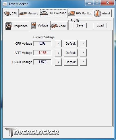
| Core Voltage | Stock VID ~ +1.26V in 0.02V increments CPU undervoltage offered Stock VID -0.02V ~ -0.08V in 0.02V increments |
| CPU Vdroop Compensation | Enabled/Disabled |
| CPU Clock Multiplier | Dependant on Processor, all available multipliers supported |
| DRAM Voltage DDR3 | Auto, 1.30V ~ 1.55VV in 0.05V ~ 0.1V increments, then 1.50V ~ 2.545V in 0.015V increments (1.50V base) |
| DRAM Timing Control | tCL, tRCD, tRP, tRAS, + 8 Additional Timings |
| DRAM Command Rate | Auto, 1N and 2N |
| PCH Voltage | Auto, 1.10V ~ 1.25V in .05V increments, 1.05V Base |
| CPU VTT (Uncore) Voltage | 1.15V ~ 2.08V in 0.015V increments |
| CPU PLL Voltage | 1.1V ~ 2.03V in 0.15V increments, 1.81V Base |
| IGD VID | Stock VID ~ +0.6V in 0.02V increments |
| Memory Slots | Four 240-pin DDR3 DIMM Slots Dual-Channel Configuration Regular Unbuffered DDR3 Memory to 16GB Total |
| Expansion Slots | 1 x PCI-E 2.0 x16 Slot 1 x PCI-E 2.0 x4 Slot (running at x4, 2.5GT/s) 2 x PCI slot |
| Onboard SATA/RAID | 5 x SATA 3.0GB/s (Support NCQ, AHCI and Hot Plug) 1 x eSATA on Rear I/O |
| Onboard USB 2.0 | 10 USB 2.0 ports (6) I/O Panel, 6 via brackets |
| Onboard LAN | 1 x Realtek 8111DL Gigabit LAN (PCI-E x1) |
| Onboard Audio | Realtek ALC888 - 7.1 Channel HD Audio |
| Other Onboard Connectors | 1 x Print Port, 1 x Serial Port, 1 x FP Audio, 1 x Front Panel, 1 x 1394, 1 x IDE (JMB368), 1 x Power Switch, 1 x Reset Button |
| Power Connectors | ATX 24-pin, 8-pin EPS 12V |
| I/O Panel | 1 x PS/2 Keyboard 1 x PS/2 Mouse 1 x RJ45 4 x USB 2.0/1.1 1 x eSATA 1 x 1394 (LSI FW 322) 1 x Optical Toslink 1 x DVI-D 1 x HDMI 1 x VGA/D-sub 6 Audio I/O jacks |
| Fan Headers | 1 CPU + 2 Additional Headers |
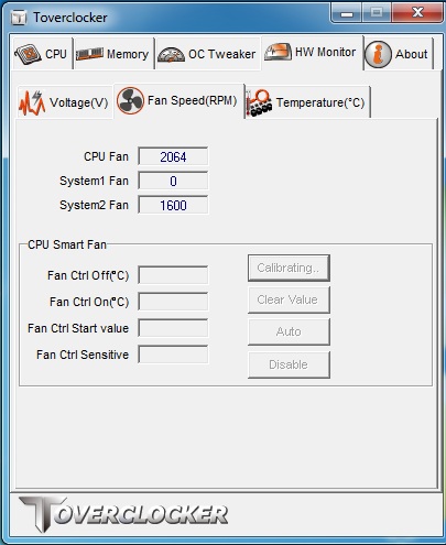
| Fan Control | Full temp/speed fan control for CPU header via BIOS or OS software No speed control for SYS Fans |
| Package Contents | 3 x SATA Cables, 1 x SATA Power Cable, 1 x User Guide, 1 x Driver/software DVD, 1 x I/O Shield |
| Board/BIOS Revisions Used | Board Rev: Ver 5.0 BIOS Files Used: H55AA107.BST |
| Form Factor | uATX (9.6 in. x 9.6 in.) |
| Warranty | 3 Years (First two years = parts and labor; third year = parts only) |
BIOSTAR's feature set is similar to ASRock's H55M-Pro in almost every way, although ASRock managed to cram a TPM header onto their board which costs less. Other than that, you get a slightly more "expensive" 4-phase VRM solution on the BIOSTAR board courtesy of MOSFETs from International Rectifier topped off with heatsinks to keep the whole shebang cool. At a guess, we'd say that BIOSTAR's implementation is limited to a maximum of around 120 amps or so (30 amps per FET), which seems to be a ballpark figure for most H55/H57 motherboards.
At the component level, you get Realtek's ALC888 for audio and Realtek 8111D LAN—commonly found on most motherboards around the $100-$300 mark. The peripheral package is made up of three SATA cables, one SATA power cable, driver DVD and rear I/O shield. As you're paying a little bit more for fewer features on the TH55XE, the inclusion of a USB bracket would have been appreciated to make use of the internal USB headers, because you've only got four connectors available on the rear I/O panel.
Software
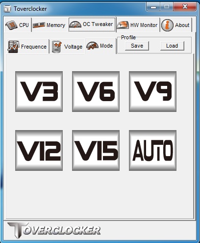
TOVERCLOCKER is included in the software package and allows voltage/bus speed changes, voltage/temperature monitoring, save/load of overclocking profiles and quick-touch overclocking for those who prefer automated methods. The system runs a quick stability test, ramps bus frequencies and repeats this process until the system crashes. Upon reboot the highest stable frequency is automatically selected and applied. Although the utility works, using the "V12" BIOS preset actually gave us a higher stable overclock (3.9GHz vs. 3.75GHz) than the automated tuning function, so we'd encourage you to delve into the "V" presets or manual overclocking instead.
BIOSTAR also includes a power saving utility called GPU (Green Power Utility) that works by shutting down PWM phases during light load conditions. Four performance related presets are available for use, although we did not notice much of a difference in power draw between the settings because Intel's CPUs draw so little power in light load conditions when C-states and SpeedStep are enabled in the BIOS. Power savings from phase shut-off are more apparent on boards that have higher phase counts and switching frequencies because you're contending against greater switching losses.
The Board
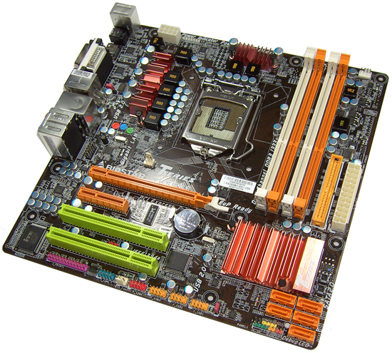


Motherboard layouts follows a similar story for most of the boards on test today, with most ports and connectors remaining within reach in commonly used configurations. One area where BIOSTAR seem to have gotten it wrong is in the placement of the PCI-E x4 slot on the TH55XE. It's placed directly below the x16 PEG slot, leaving no chance of using it if you decided to go with a discrete GPU. We're not fans of BIOSTAR's choice of PCI-E retention latches either, it can be very difficult to remove a graphics card for the primary PEG slot because the latch lever is blocked under most graphics card coolers.
Onboard PWM heatsinks are fastened with push-pins and although contact seemed good, we prefer vendors to use screw fittings wherever possible as there are instances where push pins don't seem to provide sufficient down-force for good contact. Everything else is placed in a friendly manner though, and you even get a couple of onboard power/reset buttons for open test beds (although that's an unlikely field of use for this board). Ordinarily, we'd prefer a CMOS battery location at the edge of a motherboard, but BIOSTAR's BIOS recovery routines are so good that we never had to clear CMOS, let alone remove the battery.
Overclocking
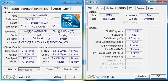
Memory overclocking results using the TH55XE are a little mixed. 4GB memory limits using high-end Elpida based modules come in at 188 BCLK (DDR3-1880 MHz):
There's a big problem with this overclock though; S3 resume is limited to between 160~165 BCLK using the 2:10 memory ratio with 4GB of memory and a high QPI multiplier, which is a real shame. It's probably something that BIOSTAR can address easily enough, but let's just say the TH55XE is not competitive in this department at present.
8GB memory overclocking results using the 2:10 memory ratio come in a little lower than boards from ASUS and Gigabyte. We topped out at DDR3-1510MHz for absolute stability:
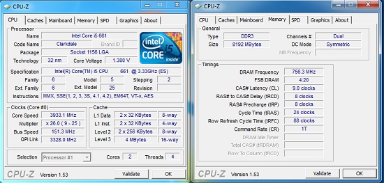
We did try a combination of 200 BCLK and the 2:8 memory ratio (DDR3-1600MHz), but did not manage to find complete stability. The Gigabyte H55M-USB3 managed to pass all of our tests with ease at the same settings.
BIOS
BIOSTAR's O.N.E menu (Overclocking Navigator Engine) is where all the action takes place with a wide variety of adjustments including the CPU Core, PLL, VTT, PCH, IGP and VDimm. Clock generator skew adjustments are also available for maximum BCLK overclocking. Overclocking profiles can be saved, loaded and individually named in one of the available 10 slots. A built in BIOS flashing function is available (by pressing F12 at boot), allowing users to save and flash the BIOS from a USB or HDD easily.
Like other vendors, BIOSTAR's DRAM timing menu needs some work. Individual sub-timings lack the option of AUTO settings. To date, ASUS and Gigabyte are the only vendors providing selective automation of DRAM sub-timing functions on their H55/H57 motherboards. This is a big plus point for users that don't understand advanced DRAM timings but want to tinker with adjustments gradually.
Recovery from failed overclock settings is excellent; this is one area where BIOSTAR are the best in the business. We did not have to clear CMOS or power down the board at all to get it to recover from a failed overclock; no other vendor seems to get this area of functionality completely right.
A selection of three automated overclocking presets are also available, taking CPUs up to 145 BCLK using conservative voltage increases and memory timings allowing for a quick stable overclock without having to get down and dirty with a multitude of BIOS settings.
Fan control is only available for the CPU fan header (via BIOS/TOVERCLOCKER/TPower), offering full temperature range and speed control. Unfortunately, the SYS fan headers cannot be controlled at all and remain "full-on" all the time.


56 Comments
View All Comments
ltcommanderdata - Tuesday, April 6, 2010 - link
I don't know if you are still monitoring this article's comments, but I was wondering if you have any idea if the latest Gigabyte H57M-USB3 F5 BIOS fixes the AHCI problems you were reporting? I am looking for a mATX motherboard with USB 3.0 and this motherboard with it's PCIe x4 slot that could be useful for a future USB 3.0/6Gps SATA expansion card seems like a good option if it's niggling issues have been worked out.RadMos - Wednesday, April 28, 2010 - link
The ECS H55H-V1.0, convince me. It has the best price and everything I need. A PC for my wife, is economic and profitable MB. It is not behind the other more expensive solutions. I just have to choose the correct CPU.hq5 - Friday, April 30, 2010 - link
How to modify the registry after installation to enable AHCI drivers on Gigabyte H57M-USB3 ?thx
taipeidman - Monday, June 14, 2010 - link
Hi Rajinder,Do you know the difference between the two fabrication revisions?
As a solution provider, I'm in direct contact with Gigabyte sales in my region.
They tell me:
"We have an unique power design of USB port to charge iphone/ipad from S1 to S5 mode. Rev. 2.0 one improves the convenience. But I ensure there is no difference of functions.
Please consider this a running change."
however, as a hardware Engineer, I see 1.0 -> 2.0 as a major revision increment, as opposed of 1.0 ->1.1.
If you look at the pictures of the GA-H57-USB3 rev1 and rev2 you can see a different IC (upper left of picture) installed on the boards between the revisions.
rev1 - http://www.gigabyte.com.tw/products/product-page.a...
- http://www.gigabyte.com.tw/fileupload/product/2/33...
rev2 - http://www.gigabyte.com.tw/products/product-page.a...
- http://www.gigabyte.com.tw/fileupload/product/2/34...
I'm asking here, if anyone knows...
I don't have the board in hand yet and the sales tells me he will supply a rev1 board.
This is why I'm asking
any thoughts?
if you still have the GA-H57M-USB3 on hand what revision do you have and can you tell me the
chip part number (just under the "Designed in Taiwan" on the upper left of the picture)
Taipeidman...
willsonjone - Tuesday, March 22, 2011 - link
Samsung, a respected brand keeps introducing mobile phones that match today’s speed and technology. Samsung has gone great lengths this time as it has received impressive reviews for its new Galaxy S 4G which happens to be the first 4G Phone with 21+ Mbps speeds.Samsung Galaxy S 4G
willsonjone - Tuesday, March 22, 2011 - link
HELLO