The RV870 Story: AMD Showing up to the Fight
by Anand Lal Shimpi on February 14, 2010 12:00 AM EST- Posted in
- GPUs
Process vs. Architecture: The Difference Between ATI and NVIDIA
Ever since NV30 (GeForce FX), NVIDIA hasn’t been first to transition to any new manufacturing process. Instead of dedicating engineers to process technology, NVIDIA chooses to put more of its resources into architecture design. The flipside is true at ATI. ATI is much less afraid of new process nodes and thus devotes more engineering resources to manufacturing. Neither approach is the right one, they both have their tradeoffs.
NVIDIA’s approach means that on a mature process, it can execute frustratingly well. It also means that between major process boundaries (e.g. 55nm to 40nm), NVIDIA won’t be as competitive so it needs to spend more time to make its architecture more competitive. And you can do a lot with just architecture alone. Most of the effort put into RV770 was architecture and look at what it gave ATI compared to the RV670.
NVIDIA has historically believed it should let ATI take all of the risk jumping to a new process. Once the process is mature, NVIDIA would switch over. That’s great for NVIDIA, but it does mean that when it comes to jumping to a brand new process - ATI has more experience. Because ATI puts itself in this situation of having to jump to an unproven process earlier than its competitor, ATI has to dedicate more engineers to process technology in order to mitigate the risk.
In talking to me Carrell was quick to point out that moving between manufacturing processes is not a transition. A transition implies a smooth gradient from one technology to another. But moving between any major transistor nodes (e.g. 55nm to 45nm, not 90nm to 80nm) it’s less of a transition and more of a jump. You try to prepare for the jump, you try your best to land exactly where you want to, but once your feet leave the ground there’s very little to control where you end up.
Any process node jump involves a great deal of risk. The trick as a semiconductor manufacturer is how you minimize that risk.
At some point, both manufacturers have to build chips on a new process node otherwise they run the risk of becoming obsolete. If you’re more than one process generation behind, it’s game over for you. The question is, what type of chip do you build on a brand new process?
There are two schools of thought here: big jump or little jump. The size refers to the size of the chip you’re using in the jump.
Proponents of the little jump believe the following. In a new process, the defect density (number of defects per unit area on the wafer) isn’t very good. You’ll have a high number defects spread out all over the wafer. In order to minimize the impact of high defect density, you should use a little die.
If we have a wafer that has 100 defects across the surface of the wafer and can fit 1000 die on the wafer, the chance that any one die will be hit with a defect is only 10%.
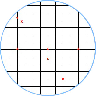
A hypothetical wafer with 7 defects and a small die. Individual die are less likely to be impacted by defects.
The big jump is naturally the opposite. You use a big die on the new process. Now instead of 1000 die sharing 100 defects, you might only have 200 die sharing 100 defects. If there’s an even distribution of defects (which isn’t how it works), the chance of a die being hit with a defect is now 50%.
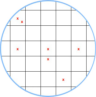
A hypothetical wafer with 7 defects and a large die.
Based on yields alone, there’s no reason you’d ever want to do a big jump. But there is good to be had from the big jump approach.
The obvious reason to do a big jump is if the things you’re going to be able to do by making huge chips (e.g. outperform the competition) will net you more revenue than if you had more of a smaller chip.
The not so obvious, but even more important reason to do a big jump is actually the reason most don’t like the big jump philosophy. Larger die are more likely to expose process problems because they will fail more often. With more opportunity to fail, you get more opportunity to see shortcomings in the process early on.
This is risky to your product, but it gives you a lot of learning that you can then use for future products based on the same process.


132 Comments
View All Comments
tomoyo - Monday, February 15, 2010 - link
Another awesome article about the real situation behind the hardware from you Anand! I was on the USS Hornet and wish I had talked to you, but it was a great time nonetheless. It's interesting the change in their thought process between the RV770 and RV870, I hope they keep the winning streak up for the next refresh cycle (which hopefully will stay on the market bulges).WT - Monday, February 15, 2010 - link
*sigh* ^^^There's always one in the crowd.
Take care in the fact that you are the only person who hasn't enjoyed this read.
MegaManX4 - Monday, February 15, 2010 - link
Reminds me much of the Anglo-Saxon "documantaries", where it is always of tertiary relevance WHAT is actually discussed, but it is always of utmost interest how the responsible person "feels" about what he is just seeing, other than just stating the facts.There seems to be a huge crowd vowing for that kind of journalism, Whatever pleases the canaille.
"Jedem das Seine" or "to each his own" then
MegaManX4 - Monday, February 15, 2010 - link
This was actually the worst article i have ever read at anandtech. I know that you Americans always strive for emotionally .Driven stories, but this outright borders on silly exaggeration."Heroes of our Industry", what a Schmalz.
Also, if one would take the real informations presented in that article, it wouldn't justify even a 2 Page Article, let alone that 11 Page behemoth.
They are engineers, they do their jobs. Nothing more, nothing less.
Greetings from Germany
blowfish - Monday, February 15, 2010 - link
hmm, with an attitude like that you'll never get past middle management!Like most here, I loved this article. Anand obviously has the friendship and respect of some very senior players, and we were treated to some great insights into how things work at AMD ATI.
As the reader, you can choose to read or not read the article, simple as that. Maybe you should up your medication.
MegaManX4 - Monday, February 15, 2010 - link
unreasonable polemicpmonti80 - Monday, February 15, 2010 - link
You are the one being unreasonable. This may not be a "scientifically written" article, but no one is claiming it to be. And that's the reason this article is so interesting.saiga6360 - Thursday, February 18, 2010 - link
Apparently German engineers are just soulless robots. His confusion is understandable.BelardA - Monday, February 15, 2010 - link
I enjoyed this article even more than the RV770. I do recommend that everyone read that one too.Kind of shocking that Nvidia didn't use that info from the RV770 article to learn to NOT make big GPUs like the GTX 2xx. yeah yeah, it takes 2-4 years to design a chip.
I thank ATI (and AMD) for not playing marketing games like Nvidia does... I think they have a bigger marketing department than engineers nowadays. They started with the GF2-MX 400 & GF4-MX cards (which were re-labeled updated GF2 cards that were not up to GF3 standards)... but the latest cluster-muck of Nvidia products is nothing but a mess. 8800 re-badged as a 9800 re-badged into the gts 250. Code-name of NVxx go to G80 to G92 to G100. The GT-1xx products that are actually low-end 9xxx products, same with most G200 & G300. I'm not going to be surprised when the GTX 285 gets renamed into the GTS450 at $200! I've seen people who bought the GTS250 and post on the internet "why isn't my new gts250 much faster than my old 8800GT"... because you bought a faster version of your card and thought it was something new. Wow, 3 years with 3 names for the same product, that is marketing.
ATI does good with the entire 4000 series being DX 10.1 products and 5000s are DX11. (Does anyone really use HD-5xxx?) It doesn't feel like ATI is pulling our chain with their products.
AMD should be learning from ATI, they are getting better with CPUs - 2 years late, but AMD CPUs are now faster than Core2 and compete well against the lower end intel i-confused model CPUs. There is still room for improvement which was recommend to them some time ago, but AMD is just going to come out with a new design for next year. But had AMD tweaked their CPUs a bit for another 10~20% performance, they'd be up there with i7s.
I hope in the next ATI GPU, some form of Physics engine is added to go up against nvidia's PhsyX. But perhaps that'll be part of DX12... but Microsoft no longer supports Games for Windows.
Actually, with more and more games going ONLY to consoles, I don't think the need for high-end gaming cards will be needed anymore in the next few years. If there are no games, who needs a $300 3D Gaming card?
Zink - Monday, February 15, 2010 - link
Would also like to say great article. I can't wait for new distributed computing cores come out optimized for ATI's architectures.