Biostar TPower i55 – Super Middle Weight Contender
by Rajinder Gill on November 25, 2009 12:00 PM EST- Posted in
- Motherboards
Board Layout and Features
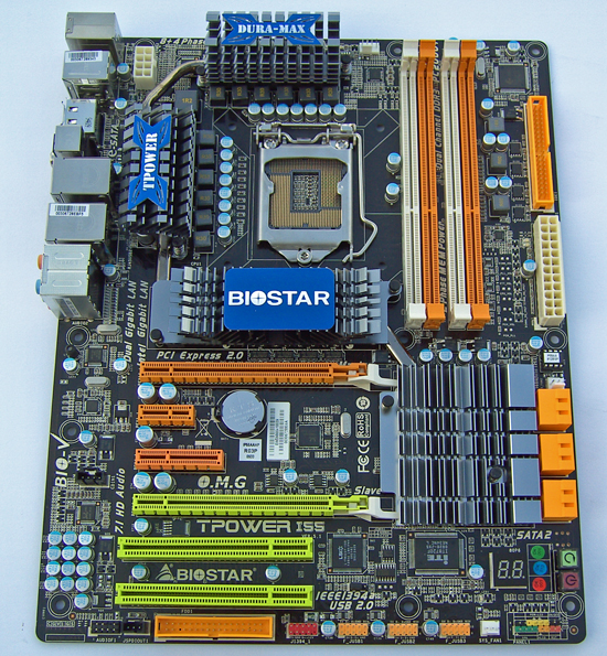
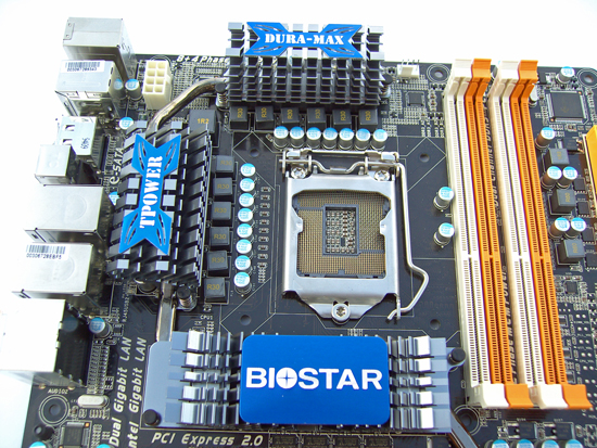
The heatsinks bearing the TPower and DURA-MAX logos provide cooling for the 8-phase uPI CPU PWM circuit, with an additional 4 phase supply for VTT (the integrated memory controller). The IR FET’s are specified at around 30 amps each, which should allow for ample overclocking headroom. The two CPU PWM heatsinks are connected by a heatpipe which also links to the BIOSTAR logo heatsink you see in the bottom of the picture. This pipe extends further to the PCH heatsink, allowing the entire assembly to be cooled with a single fan. All heatsinks are fastened with push-pins rather than screw fittings, although we found contact pressure was sufficient in this instance.
Despite the bulk used in these heatsinks, were going to recommend users to apply active cooling across the central heatsink when overclocking, especially if ramping PWM switching frequencies for heavy load testing. On the subject of heavy loads; BIOSTAR is using revised FOXCONN sockets on their boards. We’ve had no socket related problems during the course of this review and have not heard of any user reports thus far using BIOSTAR boards.
We’re a little surprised to find that there are only three onboard fan headers, one of which is assigned to the CPU. This leaves two (actually one) additional headers for active board cooling should high temperatures become a hindrance to overclocking. Do note; the SYS_FAN 2 header at the right side of the board will not be accessible if you plug a long GPU into the primary PEG slot. We’d like to have seen BIOSTAR put a little more time and consideration with regards to the number of headers and their placement on this motherboard given the target audience.
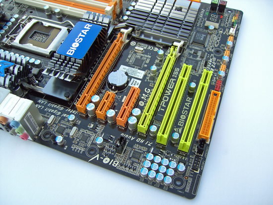
Expansion slot layout from the top down is comprised of, PCI/e x16 (x8 if the second x16 slot is filled), PCI/e x1, PCI/e x4, PCI/e x8 and two PCI slots at the bottom. You lose access to the PCI/ex 1 slot as soon as you put a GPU with a dual slot cooler in the first PEG slot, although you can use the PCI/e x4 slot instead. Running dual GPU’s will also limit users to one PCI slot, although we don’t see that as a huge deal breaker these days.
While we’re on the subject of expansion slots, we found the PCI/e retention latches to be a pain when trying to remove our 4870X2 GPU from the board. The lever does not protrude far enough to allow access easily, especially if the board is placed in a case. We had to use a set of long-nose pliers to grab the latch and force it downwards so that we could remove the GPU from the slot.
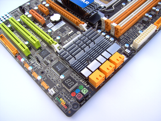
Six right angle SATA ports are available via the Intel P55 PCH. A LED hex post code reader and power/reset switches are located in the lower right corner for open test bed users. A single DIL socket BIOS chip is located above the SATA ports, while the associated CMOS clear jumper is located to the right of the last PCI slot. CMOS clear access is certainly going to be hampered somewhat if the last PCI slot is occupied, but we never needed it. Unfortunately there is no rear I/O panel CMOS clear switch, which will leave users pulling side panels off cases should the board fail to post after changing BIOS settings.
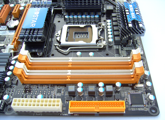
ATX 12V and IDE connectors are placed along the right edge of the board. A full spread of voltage reading pads are provided, and located between the ATX 12V connecter and the last DIMM slot. DIMM voltage is supplied by a 2-phase PWM circuit, which is pretty much the norm for boards in this price range and should certainly be more than adequate for the platform.
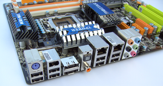
Rear I/O options include: 1 PS/2, 8 USB, 2 E-SATA, 1 IEEE-1394a, 2 RJ45 LAN, 1 S/PDIF & 1 Optical out and finally 6 AUDIO out jacks (Realtek ALC888).


39 Comments
View All Comments
Joepublic2 - Thursday, November 26, 2009 - link
Rajinder, is there any way to differentiate the new foxconn sockets from the old (serial/part numbers, a visual difference between the two)?Rajinder Gill - Thursday, November 26, 2009 - link
Hi Joe,None that I know of I'm afraid. If I do find anything out, I'll update.
regards
Raja
NumericalMethods - Thursday, November 26, 2009 - link
In your great overclocking section I see you have once again exceeded the 1.21v Intel recommended Vtt specification (by a fair amount). Is this something you would be comfortable with for 24/7 running or is this just to demonstrate the limits of the board?I have no real concept of why the Vtt spec has changed from Bloomfield but if I were running a P55 system overclocked 24/7 I suspect I couldn't expect to reach a 4+GHz overclock - it would be limited by 'safe' voltage.
Rajinder Gill - Thursday, November 26, 2009 - link
The Intel voltage specifications are given out in relation to stock operating frequencies. Increase freqeuncy and you increase power, so if you're really following Intel guidelines, then you need to observe stock operating frequencies too.There is no definative answer to what kind of degredation a CPU will experience due to elevated voltage/current long term. One can assume that the degredation will be faster, but whether or not that will be a factor for the end-user is another matter. Of course, too much voltage is certainly asking for trouble. We generally run stuff just to show what the board can do. At least it answers the question for people who like to push hard. At the same time, if the board is stable at higher operating frequencies, the more sensible stuff is ceratinly possible.
regards
Raja
Absolution75 - Thursday, November 26, 2009 - link
I always find that the most relevant information to me is left out of every motherboard review.Benchmarks for motherboards are always very similar, in fact, they are so similar that in my opinion, aren't worth mentioning. If there is a strange issue with USB speeds being low (which I've seen before), then that probably is the only benchmark that really needs any type of graph. Do people really care if the board A gets a 1KBPS higher score on the network test than board B? I'm sure this is well within the margin of error of the test anyway. This may be what you're getting at when you guys have switched the conclusion to the first page of the review, which I thought was a good decision.
Relevant information that always seems to be missing:
1) Are the fan headers able to be controlled by bios? If so, how and how well? Can they all be controlled or just a few? Sometimes it specifies, but it fails to provide any real details.
2) The audio chip. Realtek did a wonderful job at creating 'optional' features on a few of their codec’s. I bought the MSI P55-GD65 board on launch date and assumed it could do real time DDL encoding (like my old gigabyte P45-UD3P which uses the same audio codec), little did I know, that this optional feature is disabled. Apparently 'true blue ray audio' doesn't really mean much. A simple paragraph about the audio chip's capabilities would be nice. Especially since some motherboards use VIA's codec’s which tend to be even more confusing than Realtek's.
3) Strange things such as mentioning who makes the chip for the NIC and other random things would be nice. For some reason, I have a good bias towards Marvell NICs. This information seems to be included more often lately :D
4) Information about how board features are integrated into the motherboard. Is that gigabyte NIC running off a PCI-E lane or PCI?
5) Useful information about strange features such TPM headers (which you made no mention of in the MSI P55-GD65).
Specifically for this review, it is said that this board is trying to compete with the MSI P55-GD65 and you say it has an advantage even though it is more expensive ($25-$45 more). How though? It is never really said. Both boards perform identically (in fact, probably any P55 board will perform identically to another. . .) and both have similar layouts. The MSI board has 1 more PCI-E slot along with an open slot PCI-E x4. How is this not an advantage? Both have dual NICs, 2 more SATA2 ports (with the MSI board having a better solution imo - the single blue slot on the board is useful for a disk drive leaving the entire 6x SATA2 ports on the P55 chipset for some type(s) or RAID) and digital audio.
Also, a complete guess, but board designers probably still include the floppy drive header just because its included in the chip they use for IDE and additional SATA (maybe jmicron doesn't make a chip that is just IDE/SATA instead of IDE/SATA/floppy), or maybe they just cost the same. . .
ereavis - Wednesday, December 9, 2009 - link
"Test Setup" is a big missing for me. What are you calling an "Intel P55" on these charts or all the Intel P55 motherboards from $90-$240 the same performance?g725s - Wednesday, December 2, 2009 - link
Cool conclusion on first page. Keep it up!Rajinder Gill - Wednesday, December 2, 2009 - link
Some seem to like it while others are not impressed (check the firs page of comments). I'll probably do some kind of exec front page summary in the future.later
Raja
treesloth - Monday, December 7, 2009 - link
FWIW, I like it. Interestingly to me, it's essentially the same layout and format that I use for my testing an analysis at work, so I actually feel sort of vindicated. :-)treesloth - Monday, December 7, 2009 - link
FWIW, I like it. Interestingly to me, it's essentially the same layout and format that I use for my testing an analysis at work, so I actually feel sort of vindicated. :-)