NVIDIA's Fermi: Architected for Tesla, 3 Billion Transistors in 2010
by Anand Lal Shimpi on September 30, 2009 12:00 AM EST- Posted in
- GPUs
A Different Sort of Launch
Fermi will support DirectX 11 and NVIDIA believes it'll be faster than the Radeon HD 5870 in 3D games. With 3 billion transistors, it had better be. But that's the extent of what NVIDIA is willing to talk about with regards to Fermi as a gaming GPU. Sorry folks, today's launch is targeted entirely at Tesla.
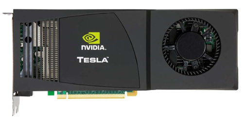
A GeForce GTX 280 with 4GB of memory is the foundation for the Tesla C1060 cards
Tesla is NVIDIA's High Performance Computing (HPC) business. NVIDIA takes its consumer GPUs, equips them with a ton of memory, and sells them in personal or datacenter supercomputers called Tesla supercomputers or computing clusters. If you have an application that can run well on a GPU, the upside is tremendous.
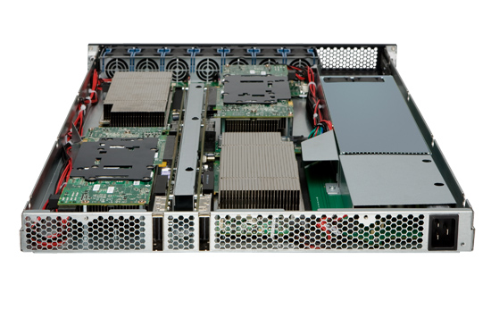
Four of those C1060 cards in a 1U chassis make the Tesla S1070. PCIe connects the S1070 to the host server.
NVIDIA loves to cite examples of where algorithms ported to GPUs work so much better than CPUs. One such example is a seismic processing application that HESS found ran very well on NVIDIA GPUs. It migrated a cluster of 2000 servers to 32 Tesla S1070s, bringing total costs down from $8M to $400K, and total power from 1200kW down to 45kW.
| HESS Seismic Processing Example | Tesla | CPU |
| Performance | 1 | 1 |
| # of Machines | 32 Tesla S1070s | 2000 x86 servers |
| Total Cost | ~$400K | ~$8M |
| Total Power | 45kW | 1200kW |
Obviously this doesn't include the servers needed to drive the Teslas, but presumably that's not a significant cost. Either way the potential is there, it's just a matter of how many similar applications exist in the world.
According to NVIDIA, there are many more cases like this in the market. The table below shows what NVIDIA believes is the total available market in the next 18 months for these various HPC segments:
| Processor | Seismic | Supercomputing | Universities | Defence | Finance |
| GPU TAM | $300M | $200M | $150M | $250M | $230M |
These figures were calculated by looking at the algorithms used in each segment, the number of Hess-like Tesla installations that can be done, and the current budget for non-GPU based computing in those markets. If NVIDIA met its goals here, the Tesla business could be bigger than the GeForce one. There's just one problem:
As you'll soon see, many of the architectural features of Fermi are targeted specifically for Tesla markets. The same could be said about GT200, albeit to a lesser degree. Yet Tesla accounted for less than 1.3% of NVIDIA's total revenue last quarter.
Given these numbers it looks like NVIDIA is building GPUs for a world that doesn't exist. NVIDIA doesn't agree.
The Evolution of GPU Computing
When matched with the right algorithms and programming efforts, GPU computing can provide some real speedups. Much of Fermi's architecture is designed to improve performance in these HPC and other GPU compute applications.
Ever since G80, NVIDIA has been on this path to bring GPU computing to reality. I rarely get the opportunity to get a non-marketing answer out of NVIDIA, but in talking to Jonah Alben (VP of GPU Engineering) I had an unusually frank discussion.
From the outside, G80 looks to be a GPU architected for compute. Internally, NVIDIA viewed it as an opportunistic way to enable more general purpose computing on its GPUs. The transition to a unified shader architecture gave NVIDIA the chance to, relatively easily, turn G80 into more than just a GPU. NVIDIA viewed GPU computing as a future strength for the company, so G80 led a dual life. Awesome graphics chip by day, the foundation for CUDA by night.
Remember that G80 was hashed out back in 2002 - 2003. NVIDIA had some ideas of where it wanted to take GPU computing, but it wasn't until G80 hit that customers started providing feedback that ultimately shaped the way GT200 and Fermi turned out.
One key example was support for double precision floating point. The feature wasn't added until GT200 and even then, it was only added based on computing customer feedback from G80. Fermi kicks double precision performance up another notch as it now executes FP64 ops at half of its FP32 rate (more on this later).
While G80 and GT200 were still primarily graphics chips, NVIDIA views Fermi as a processor that makes compute just as serious as graphics. NVIDIA believes it's on a different course, at least for the short term, than AMD. And you'll see this in many of the architectural features of Fermi.


415 Comments
View All Comments
Inkie - Saturday, October 3, 2009 - link
Not that I really want to support SD here, but there was working silicon there. It's kind of weird that many sites fail to mention this. Instead, they focus on the mockup.SiliconDoc - Thursday, October 1, 2009 - link
Go read a few articles on how a card is developed, and you'll have the timeline, you red rooster retard.I mean really, I'm talking to ignoramussed spitting cockled mooks.
Please, the articles are right here on your red fan website, so go have a read since it's so important to you how people act when your idiotic speculation is easily and absolutely 100% incorrect, and it's PROVEABLE, the facts are already IN.
gx80050 - Friday, October 2, 2009 - link
You're a fucking friendless loser who should have died on 9/11. Fucking cuntmonomer - Friday, October 2, 2009 - link
In reply to your original link, here's a retraction, of sorts:http://www.fudzilla.com/content/view/15798/1/">http://www.fudzilla.com/content/view/15798/1/
The card Nvidia showed everyone, and said was Fermi is in fact a mock-up. Oh well.
silverblue - Thursday, October 1, 2009 - link
What facts? What framerates can it manage in Crysis? What scores in 3DMark? How good it is at F@H?Link us, so we can all be shown the errors of our ways. It's obvious that GT300 has been benchmarked, or at least, it's only obvious to you simply because the rest of us are on a different planet.
You call people idiots, and then when they reply in a sensible manner, you conveniently forget all that and call them biased (along with multiple variations on the red rooster theme). You're like a scratched vinyl record and it's about time you got off this site if you hate its oh-so-anti-nVidia stance that doesn't actually exist except in your head.
Prove us wrong! Please! I want to see those GT300 benchmarks! Evidence that Anandtech are so far up AMD's rear end that nothing else is worth reporting on fairly!
Zool - Thursday, October 1, 2009 - link
GTX285 had 32 ROPs and 80 TMUs for aorund the same bandwith like 5870 with same 32 ROPs and 80 TMUs. Dont be stupid. GTX will surely need more ROPs and TMUs if they want to keep up with graphic even with the GPGPU bloat.Totally - Wednesday, September 30, 2009 - link
it's 225GB/s not 230.4/s230400/1024 = 225
I'm afraid your bad at math.
Lightnix - Thursday, October 1, 2009 - link
Nope, just really bad at remembering that those prefixes mean 1024 at like 1 in the morning.Lonyo - Wednesday, September 30, 2009 - link
You assume that they will use GDDR5 clocked at the same speed as ATI.They could use higher clocked GDDR5 (meaning even more bandwidth), or lower clocked GDDR5 (meaning less bandwidth).
There's no bandwidth comparison because 1) it's meaningless and 2) it's impossible to make an absolute comparison.
NV will have 50% more bandwidth if the speed of the RAM is the same, but it doesn't have to be the same, it could be higher, or lower, so you can't say what absolute numbers NV will have.
I could make a graph showing equal bandwidth between the two cards even though NV has a bigger bus, or I could make one showing NV having two times the bandwidth despite only a 50% bigger bus.
Both could be valid, but both would be speculative.
Calin - Thursday, October 1, 2009 - link
Also, there could be a chance that the Fermi chip doesn't need/use much more bandwidth than the GT200. Available bandwidth does not performance make