NVIDIA's Fermi: Architected for Tesla, 3 Billion Transistors in 2010
by Anand Lal Shimpi on September 30, 2009 12:00 AM EST- Posted in
- GPUs
The graph below is one of transistor count, not die size. Inevitably, on the same manufacturing process, a significantly higher transistor count translates into a larger die size. But for the purposes of this article, all I need to show you is a representation of transistor count.
![]()
See that big circle on the right? That's Fermi. NVIDIA's next-generation architecture.
NVIDIA astonished us with GT200 tipping the scales at 1.4 billion transistors. Fermi is more than twice that at 3 billion. And literally, that's what Fermi is - more than twice a GT200.
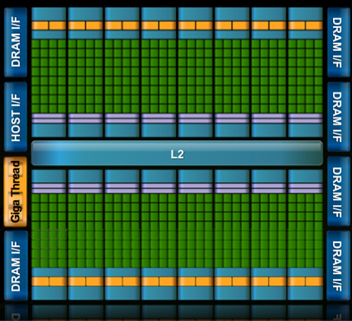
At the high level the specs are simple. Fermi has a 384-bit GDDR5 memory interface and 512 cores. That's more than twice the processing power of GT200 but, just like RV870 (Cypress), it's not twice the memory bandwidth.
The architecture goes much further than that, but NVIDIA believes that AMD has shown its cards (literally) and is very confident that Fermi will be faster. The questions are at what price and when.
The price is a valid concern. Fermi is a 40nm GPU just like RV870 but it has a 40% higher transistor count. Both are built at TSMC, so you can expect that Fermi will cost NVIDIA more to make than ATI's Radeon HD 5870.
Then timing is just as valid, because while Fermi currently exists on paper, it's not a product yet. Fermi is late. Clock speeds, configurations and price points have yet to be finalized. NVIDIA just recently got working chips back and it's going to be at least two months before I see the first samples. Widespread availability won't be until at least Q1 2010.
I asked two people at NVIDIA why Fermi is late; NVIDIA's VP of Product Marketing, Ujesh Desai and NVIDIA's VP of GPU Engineering, Jonah Alben. Ujesh responded: because designing GPUs this big is "fucking hard".
Jonah elaborated, as I will attempt to do here today.


415 Comments
View All Comments
Inkie - Saturday, October 3, 2009 - link
Not that I really want to support SD here, but there was working silicon there. It's kind of weird that many sites fail to mention this. Instead, they focus on the mockup.SiliconDoc - Thursday, October 1, 2009 - link
Go read a few articles on how a card is developed, and you'll have the timeline, you red rooster retard.I mean really, I'm talking to ignoramussed spitting cockled mooks.
Please, the articles are right here on your red fan website, so go have a read since it's so important to you how people act when your idiotic speculation is easily and absolutely 100% incorrect, and it's PROVEABLE, the facts are already IN.
gx80050 - Friday, October 2, 2009 - link
You're a fucking friendless loser who should have died on 9/11. Fucking cuntmonomer - Friday, October 2, 2009 - link
In reply to your original link, here's a retraction, of sorts:http://www.fudzilla.com/content/view/15798/1/">http://www.fudzilla.com/content/view/15798/1/
The card Nvidia showed everyone, and said was Fermi is in fact a mock-up. Oh well.
silverblue - Thursday, October 1, 2009 - link
What facts? What framerates can it manage in Crysis? What scores in 3DMark? How good it is at F@H?Link us, so we can all be shown the errors of our ways. It's obvious that GT300 has been benchmarked, or at least, it's only obvious to you simply because the rest of us are on a different planet.
You call people idiots, and then when they reply in a sensible manner, you conveniently forget all that and call them biased (along with multiple variations on the red rooster theme). You're like a scratched vinyl record and it's about time you got off this site if you hate its oh-so-anti-nVidia stance that doesn't actually exist except in your head.
Prove us wrong! Please! I want to see those GT300 benchmarks! Evidence that Anandtech are so far up AMD's rear end that nothing else is worth reporting on fairly!
Zool - Thursday, October 1, 2009 - link
GTX285 had 32 ROPs and 80 TMUs for aorund the same bandwith like 5870 with same 32 ROPs and 80 TMUs. Dont be stupid. GTX will surely need more ROPs and TMUs if they want to keep up with graphic even with the GPGPU bloat.Totally - Wednesday, September 30, 2009 - link
it's 225GB/s not 230.4/s230400/1024 = 225
I'm afraid your bad at math.
Lightnix - Thursday, October 1, 2009 - link
Nope, just really bad at remembering that those prefixes mean 1024 at like 1 in the morning.Lonyo - Wednesday, September 30, 2009 - link
You assume that they will use GDDR5 clocked at the same speed as ATI.They could use higher clocked GDDR5 (meaning even more bandwidth), or lower clocked GDDR5 (meaning less bandwidth).
There's no bandwidth comparison because 1) it's meaningless and 2) it's impossible to make an absolute comparison.
NV will have 50% more bandwidth if the speed of the RAM is the same, but it doesn't have to be the same, it could be higher, or lower, so you can't say what absolute numbers NV will have.
I could make a graph showing equal bandwidth between the two cards even though NV has a bigger bus, or I could make one showing NV having two times the bandwidth despite only a 50% bigger bus.
Both could be valid, but both would be speculative.
Calin - Thursday, October 1, 2009 - link
Also, there could be a chance that the Fermi chip doesn't need/use much more bandwidth than the GT200. Available bandwidth does not performance make