NVIDIA's Fermi: Architected for Tesla, 3 Billion Transistors in 2010
by Anand Lal Shimpi on September 30, 2009 12:00 AM EST- Posted in
- GPUs
A Different Sort of Launch
Fermi will support DirectX 11 and NVIDIA believes it'll be faster than the Radeon HD 5870 in 3D games. With 3 billion transistors, it had better be. But that's the extent of what NVIDIA is willing to talk about with regards to Fermi as a gaming GPU. Sorry folks, today's launch is targeted entirely at Tesla.
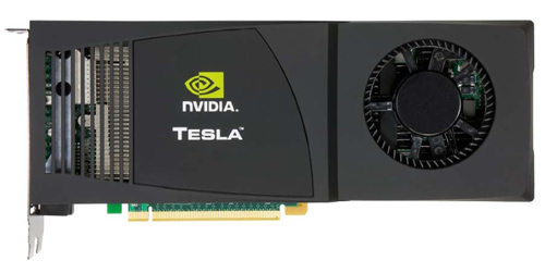
A GeForce GTX 280 with 4GB of memory is the foundation for the Tesla C1060 cards
Tesla is NVIDIA's High Performance Computing (HPC) business. NVIDIA takes its consumer GPUs, equips them with a ton of memory, and sells them in personal or datacenter supercomputers called Tesla supercomputers or computing clusters. If you have an application that can run well on a GPU, the upside is tremendous.
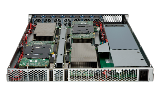
Four of those C1060 cards in a 1U chassis make the Tesla S1070. PCIe connects the S1070 to the host server.
NVIDIA loves to cite examples of where algorithms ported to GPUs work so much better than CPUs. One such example is a seismic processing application that HESS found ran very well on NVIDIA GPUs. It migrated a cluster of 2000 servers to 32 Tesla S1070s, bringing total costs down from $8M to $400K, and total power from 1200kW down to 45kW.
| HESS Seismic Processing Example | Tesla | CPU |
| Performance | 1 | 1 |
| # of Machines | 32 Tesla S1070s | 2000 x86 servers |
| Total Cost | ~$400K | ~$8M |
| Total Power | 45kW | 1200kW |
Obviously this doesn't include the servers needed to drive the Teslas, but presumably that's not a significant cost. Either way the potential is there, it's just a matter of how many similar applications exist in the world.
According to NVIDIA, there are many more cases like this in the market. The table below shows what NVIDIA believes is the total available market in the next 18 months for these various HPC segments:
| Processor | Seismic | Supercomputing | Universities | Defence | Finance |
| GPU TAM | $300M | $200M | $150M | $250M | $230M |
These figures were calculated by looking at the algorithms used in each segment, the number of Hess-like Tesla installations that can be done, and the current budget for non-GPU based computing in those markets. If NVIDIA met its goals here, the Tesla business could be bigger than the GeForce one. There's just one problem:
As you'll soon see, many of the architectural features of Fermi are targeted specifically for Tesla markets. The same could be said about GT200, albeit to a lesser degree. Yet Tesla accounted for less than 1.3% of NVIDIA's total revenue last quarter.
Given these numbers it looks like NVIDIA is building GPUs for a world that doesn't exist. NVIDIA doesn't agree.
The Evolution of GPU Computing
When matched with the right algorithms and programming efforts, GPU computing can provide some real speedups. Much of Fermi's architecture is designed to improve performance in these HPC and other GPU compute applications.
Ever since G80, NVIDIA has been on this path to bring GPU computing to reality. I rarely get the opportunity to get a non-marketing answer out of NVIDIA, but in talking to Jonah Alben (VP of GPU Engineering) I had an unusually frank discussion.
From the outside, G80 looks to be a GPU architected for compute. Internally, NVIDIA viewed it as an opportunistic way to enable more general purpose computing on its GPUs. The transition to a unified shader architecture gave NVIDIA the chance to, relatively easily, turn G80 into more than just a GPU. NVIDIA viewed GPU computing as a future strength for the company, so G80 led a dual life. Awesome graphics chip by day, the foundation for CUDA by night.
Remember that G80 was hashed out back in 2002 - 2003. NVIDIA had some ideas of where it wanted to take GPU computing, but it wasn't until G80 hit that customers started providing feedback that ultimately shaped the way GT200 and Fermi turned out.
One key example was support for double precision floating point. The feature wasn't added until GT200 and even then, it was only added based on computing customer feedback from G80. Fermi kicks double precision performance up another notch as it now executes FP64 ops at half of its FP32 rate (more on this later).
While G80 and GT200 were still primarily graphics chips, NVIDIA views Fermi as a processor that makes compute just as serious as graphics. NVIDIA believes it's on a different course, at least for the short term, than AMD. And you'll see this in many of the architectural features of Fermi.


415 Comments
View All Comments
rennya - Friday, October 2, 2009 - link
Go ask the administrator to check my IP and they can verify that my IP comes from a SE Asia country. Are you accusing me of lying for claiming that I come from a nirvana where 5870 GPU is plentiful?Is that all you can do?
Fact - 5870 is not paper launch. You cannot even deny this.
Ah, BTW, English in SE Asia is the same as the ones used in America and Europe.
Totally - Friday, October 2, 2009 - link
Seriously, what are you on? It has to be some good stuff. I want some.I like how you go on and on spouting nonsense about how GT300 has 50% more theoretical bandwith, but without clock speeds there is no way to gauge how much of it will be saturated. In plain speak: Without hard numbers BANDWIDTH ALONE MEANS NOTHING. Sure nvidia has tons of road but we have no idea what they are going to drive on it.
About the 5870 being a paper launch, my best friend had his since the 30th. Day the 5850 launched, took a look over at newegg at 7 in the evening they where there available to order. And still you can order/go to the store and purchase either right now!!! That's not a paper launch. Last time I checked a paper launch is when a product goes live and it's unavailable for over a month.
lyeoh - Friday, October 2, 2009 - link
Doesn't look like good stuff to me. You'd probably get brain damage or worse.Should be banned in most countries.
SiliconDoc - Wednesday, September 30, 2009 - link
When anand posts the GD bit width and transistor count, and mem, then CLAIMS bandwith is NOT DOUBLE, it is CLEAR the very simple calculation you 3rd graders don't know is AVAILABLE.---
IT'S 240 GB !
4800x384/8 !
duhhhhhhhhhhhhhhhhhhhhhhhhhhhhhhhhhhhhhhhhhh
It's not FUD, it's just you people are so ignorant it's EASY to have the wool pulled over your eyes.
Lightnix - Wednesday, September 30, 2009 - link
4800mHz x 384 / 8 = 230400mB/s = 230.4GB/sOr 50% faster than 153GB/s - still a big gap but clearly not even nearly double.
It's not FUD, it's just you trolls are so bad at maths you can't even use a calculator to do basic arithmetic with it's EASY to have the wool pulled over your eyes.
SiliconDoc - Wednesday, September 30, 2009 - link
The author claimed not double the former GT200, sir.In the 5870 review just the other day, the 5870 had a disappointing 153+ bandwith, vs the 115 of the 4780 or 124 of the 4890.
--
So you can see with the 5870 it went up by not much.
--
In this review, the former GT200 referred to has a 112, 127, 141, or 159 bandwith, as compared to the MYSTERY # 240 for the GT300.
So the author claims in back reference to the ati card the nvidia card "also fails" to double it's predecesor.
--
I have a problem with that - since this new GT300 is gonig to be 240 bandwith, nearly 100 GB/sec more than the card the author holds up higher and gioves a massive break to, the one not being reviewed, the ati 5870.
--
It's bias, period. The author could fairly have mentioned how it will be far ahead of it's competition, and be much higher, as it's predecessor nvidia card was also much higher.
Instead, we get the cryptic BS that winds up praising ati instead of pointing out the massive LEAD this new GT300 will have in the bandiwth area.
I hope you can understand, but if you cannot, it's no wonder the author does such a thing, as it appears he can snowball plenty with it.
UNCjigga - Thursday, October 1, 2009 - link
STFU you stupid moron. There's no "bias". The 5870 has a full, in-depth, separate review with full benchmarks. The author didn't do direct comparisons because THERE IS NO CARD TO COMPARE IT WITH TODAY. FERMI ONLY EXISTS ON PAPER--the mere existence of engineering samples doesn't help this review. The author even indicated he wished he had more info to share but that's all Nvidia allowed. How about we wait until a GT300 ships before we start making final judgements, ok?SiliconDoc - Thursday, October 1, 2009 - link
Good job ignoramus.http://www.fudzilla.com/content/view/15762/1">http://www.fudzilla.com/content/view/15762/1
Oh, look at that, you're 100% INCORRECT.
Another loser idiot with insults and NOTHING ELSE but the sheepled parrot mind that was slammed into stupidity by the author of this piece.
Great job doofu.
ufon68 - Thursday, October 1, 2009 - link
Wow, you must be the biggest fanboy i've ever seen. It would be funny if it wasn't so sad you're vasting so much energy on such insignificant issue and everyone around here just thought to themselves..."what a total failure".But hey, on the bright-side, you made me jump off that fence and register, so you might not be as useless as you seem.
monomer - Thursday, October 1, 2009 - link
Wow, your proof that Fermi exists is a photo of Huang holding up a mock-up of what the new card is going to look like?If that was a real card, and engineering samples existed, why isn't it actually in a PCI-e slot running something? Why were no functioning Fermi cards actually shown at the conference? Why was the ray-tracing demo performed on a GT200?
Finally, why did Huang say that cards will be ready in "a few short months", if they are actually ready now?
You need to calm down a little. You also need to work on your reading skills and to stop making up controversies where none exist.
Yes, Anand pointed out that the memory bandwidth did not double, but in the very same sentence, he mentions that it did not double for the 5870 either.