The Real Conroe Successor: Clarkdale & All You Need to Know about Westmere
by Anand Lal Shimpi on September 24, 2009 6:00 PM EST- Posted in
- CPUs
Quad Core Performance From Two Cores?
Intel released some preliminary performance data on Clarkdale. This data wasn't run by us and is straight from Intel. It's normalized to a Core 2 Duo E8500 and also includes a Core 2 Quad Q9400. The systems used G45 graphics for the LGA-775 parts and Clarkdale on-package graphics for the LGA-1156 setup.
We don't usually look at SPEC CPU performance, but here are the results regardless:
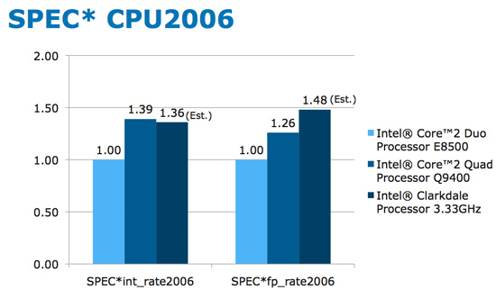
You can see that thanks to a competitive clock speed, aggressive turbo modes and Hyper Threading the 3.33GHz Clarkdale outperforms both the Q9400 and the E8500.
3DMark Vantage is of course faster on the newer platform thanks to the on-package graphics:
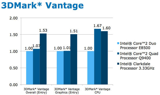
The overall performance improvement is roughly 50% in 3DMark Vantage.
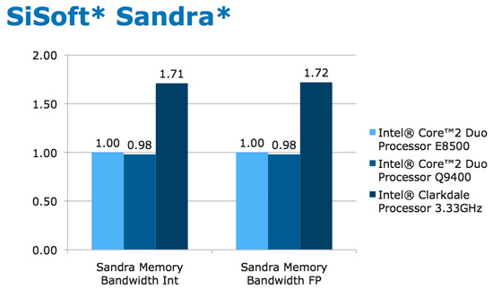
Memory bandwidth is clearly better thanks to Clarkdale's on-die dual-channel DDR3 memory controller.
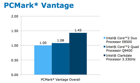
PCMark Vantage also shows a huge performance advantage on Clarkdale, however Intel mentioned that a big portion of that are the AES-NI instructions on Clarkdale accelerating one of the tests.
We'll be testing Clarkdale for ourselves later this year. It seems that this potent dual core with Hyper Threading could be a good alternative to making the quad-core jump.


96 Comments
View All Comments
jordanclock - Friday, September 25, 2009 - link
I see you're privy to data we are not seeing. Could you please share where you received this information that moving the memory controller to another chip ON THE SAME SOCKET will somehow cause pre-IMC memory latencies? We'd all like to see some actual numbers instead of sensationalist guesses.KaarlisK - Friday, September 25, 2009 - link
I remembered reading about it somewhere.It was from the benchmark here. http://global.hkepc.com/3878/page/5#view">http://global.hkepc.com/3878/page/5#view
Though the latency in this review is higher than Core 2's, which makes it suspect.
As to the why, there are smarter people than me who could answer whether there's any impact from locating the other die on the CPU package or in the chipset.
GeorgeH - Thursday, September 24, 2009 - link
Hopefully more major manufacturers will offer Mini-ITX motherboards this generation. It's nice to see at least one Intel board, but if 775 is any indication it'll be almost ridiculously feature poor.I also hope PS and case manufacturers are paying attention - the current crop of mini-ITX options is pitiful.
Mr Perfect - Saturday, September 26, 2009 - link
Absolutely.I'm impressed that the mITX has what looks to be an x16 PCIe slot on it though. In the past, Intel was always throwing a PCI or x1 slot on them. I think they where afraid that people would stop buying the bigger, more expensive boards. I know I would have.
Hopefully Anand will take a good hard look at this sector.
tomoyo - Friday, September 25, 2009 - link
No kidding! There's a total lack of good mini-itx boards with undervolting features and only one server raid case for mini-itx at all. It's sad because I'm sure a ton of people would love to make a small DIY raid nas system and not deal with the low end parts and lack of OS choice in pre-built nas systems.Aquila76 - Thursday, September 24, 2009 - link
I was going to build an HTPC soon, but if this can really bitstream TrueHD & DTS-MA on a single, low-power chip then I can wait. Next year is going to kill my wallet, but at least I can start saving now!mgl888 - Thursday, September 24, 2009 - link
What's gonna happen after 22nm? 10nm?When are we gonna hit a brick wall and what's Intel plan to do next?
Quantum computing?
Zink - Thursday, September 24, 2009 - link
It looks like there is going to be a big delay after 22nm because the thickness of certain layers in the transistors can not be scaled thinner.Check out 16nm too: http://en.wikipedia.org/wiki/22_nanometer">http://en.wikipedia.org/wiki/22_nanometer
jwilliams4200 - Thursday, September 24, 2009 - link
Each die shrink generation decreases the gate length by a factor of the square root of two (0.707), so that the die area decreases by a factor of two every shrink. To answer your questions, the gate lengths to expect are: 45nm, 32nm, 22nm, 16nm, 11nm, 8nm, 5.6nm ...As to how the lower ones can be achieved, or whether they will be achieved, I will not venture a guess.
CurseTheSky - Thursday, September 24, 2009 - link
Thank you for clarifying that. I always wondered how they determined what the next process size would be. It seemed like they picked arbitrary numbers out of a hat, but now I see that:65 / 2^(1/2) = 45.96
45 / 2^(1/2) = 31.82
32 / 2^(1/2) = 22.63
etc.