AMD's Radeon HD 5870: Bringing About the Next Generation Of GPUs
by Ryan Smith on September 23, 2009 9:00 AM EST- Posted in
- GPUs
Lower Idle Power & Better Overcurrent Protection
One aspect AMD was specifically looking to improve in Cypress over RV770 was idle power usage. The load power usage for RV770 was fine at 160W for the HD4870, but that power usage wasn’t dropping by a great deal when idle – it fell by less than half to 90W. Later BIOS revisions managed to knock a few more watts off of this, but it wasn’t a significant change, and even later designs like RV790 still had limits to their idling abilities by only being able to go down to 60W at idle.
As a consequence, AMD went about designing the Cypress with a much, much lower target in mind. Their goal was to get idle power down to 30W, 1/3rd that of RV770. What they got was even better: they came in past that target by 10%, hitting a final idle power of 27W. As a result the Cypress can idle at 30% of the power as RV770, or as compared to Cypress’s load power of 188W, some 14% of its load power.
Accomplishing this kind of dramatic reduction in idle power usage required several changes. Key among them has been the installation of additional power regulating circuitry on the board, and additional die space on Cypress assigned to power regulation. Notably, all of these changes were accomplished without the use of power-gating to shut down unused portions of the chip, something that’s common on CPUs. Instead all of these changes have been achieved through more exhaustive clock-gating (that is, reducing power consumption by reducing clock speeds), something GPUs have been doing for some time now.
The use of clock-gating is quickly evident when we discuss the idle/2D clock speeds of the 5870, which is 150mhz for the core, and 300mhz for the memory . The idle clock speeds here are significantly lower than the 4870 (550/900), which in the case of the core is the source of its power savings as compared to the 4870. As tweakers who have attempted to manually reduce the idle clocks on RV770 based cards for further power savings have noticed, RV770 actually loses stability in most situations if its core clock drops too low. With the Cypress this has been rectified, enabling it to hit these lower core speeds.
Even bigger however are the enhancements to Cypress’s memory controller, which allow it to utilize a number of power-saving tricks with GDDR5 RAM, along with other features that we’ll get to in a bit. With RV770’s memory controller, it was not capable of taking advantage of very many of GDDR5’s advanced features besides the higher bandwidth abilities. Lacking this full bag of tricks, RV770 and its derivatives were unable to reduce the memory clock speed, which is why the 4870 and other products had such high memory clock speeds even at idle. In turn this limited the reduction in power consumption attained by idling GDDR5 modules.
With Cypress AMD has implemented nearly the entire suite of GDDR5’s power saving features, allowing them to reduce the power usage of the memory controller and the GDDR5 modules themselves. As with the improvements to the core clock, key among the improvement in memory power usage is the ability to go to much lower memory clock speeds, using fast GDDR5 link re-training to quickly switch the memory clock speed and voltage without inducing glitches. AMD is also now using GDDR5’s low power strobe mode, which in turn allows the memory controller to save power by turning off the clock data recovery mechanism. When discussing the matter with AMD, they compared these changes to putting the memory modules and memory controller into a GDDR3-like mode, which is a fair description of how GDDR5 behaves when its high-speed features are not enabled.
Finally, AMD was able to find yet more power savings for Crossfire configurations, and as a result the slave card(s) in a Crossfire configuration can use even less power. The value given to us for an idling slave card is 20W, which is a product of the fact that the slave cards go completely unused when the system is idling. In this state slave cards are still capable of instantaneously ramping up for full-load use, although conceivably AMD could go even lower still by powering down the slave cards entirely at a cost of this ability.
On the opposite side of the ability to achieve such low idle power usage is the need to manage load power usage, which was also overhauled for the Cypress. As a reminder, TDP is not an absolute maximum, rather it’s a maximum based on what’s believed to be the highest reasonable load the card will ever experience. As a result it’s possible in extreme circumstances for the card to need power beyond what its TDP is rated for, which is a problem.
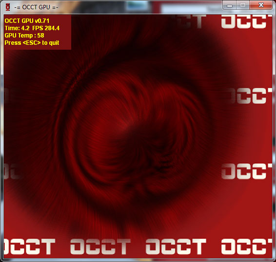
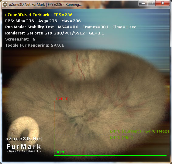
That problem reared its head a lot for the RV770 in particular, with the rise in popularity of stress testing programs like FurMark and OCCT. Although stress testers on the CPU side are nothing new, FurMark and OCCT heralded a new generation of GPU stress testers that were extremely effective in generating a maximum load. Unfortunately for RV770, the maximum possible load and the TDP are pretty far apart, which becomes a problem since the VRMs used in a card only need to be spec’d to meet the TDP of a card plus some safety room. They don’t need to be able to meet whatever the true maximum load of a card can be, as it should never happen.
Why is this? AMD believes that the instruction streams generated by OCCT and FurMark are entirely unrealistic. They try to hit everything at once, and this is something that they don’t believe a game or even a GPGPU application would ever do. For this reason these programs are held in low regard by AMD, and in our discussions with them they referred to them as “power viruses”, a term that’s normally associated with malware. We don’t agree with the terminology, but in our testing we can’t disagree with AMD about the realism of their load – we can’t find anything that generates the same kind of loads as OCCT and FurMark.
Regardless of what AMD wants to call these stress testers, there was a real problem when they were run on RV770. The overcurrent situation they created was too much for the VRMs on many cards, and as a failsafe these cards would shut down to protect the VRMs. At a user level shutting down like this isn’t a very helpful failsafe mode. At a hardware level shutting down like this isn’t enough to protect the VRMs in all situations. Ultimately these programs were capable of permanently damaging RV770 cards, and AMD needed to do something about it. For RV770 they could use the drivers to throttle these programs; until Catalyst 9.8 they detected the program by name, and since 9.8 they detect the ratio of texture to ALU instructions (Ed: We’re told NVIDIA throttles similarly, but we don’t have a good control for testing this statement). This keeps RV770 safe, but it wasn’t good enough. It’s a hardware problem, the solution needs to be in hardware, particularly if anyone really did write a power virus in the future that the drivers couldn’t stop, in an attempt to break cards on a wide scale.
This brings us to Cypress. For Cypress, AMD has implemented a hardware solution to the VRM problem, by dedicating a very small portion of Cypress’s die to a monitoring chip. In this case the job of the monitor is to continually monitor the VRMs for dangerous conditions. Should the VRMs end up in a critical state, the monitor will immediately throttle back the card by one PowerPlay level. The card will continue operating at this level until the VRMs are back to safe levels, at which point the monitor will allow the card to go back to the requested performance level. In the case of a stressful program, this can continue to go back and forth as the VRMs permit.
By implementing this at the hardware level, Cypress cards are fully protected against all possible overcurrent situations, so that it’s not possible for any program (OCCT, FurMark, or otherwise) to damage the hardware by generating too high of a load. This also means that the protections at the driver level are not needed, and we’ve confirmed with AMD that the 5870 is allowed to run to the point where it maxes out or where overcurrent protection kicks in.
On that note, because card manufacturers can use different VRMs, it’s very likely that we’re going to see some separation in performance on FurMark and OCCT based on the quality of the VRMs. The cheapest cards with the cheapest VRMs will need to throttle the most, while luxury cards with better VRMs would need to throttle little, if at all. This should make little difference in stock performance on real games and applications (since as we covered earlier, we can’t find anything that pushes a card to excess) but it will likely make itself apparent in overclocking. Overclocked cards - particularly those with voltage modifications – may hit throttle situations in normal applications, which means the VRMs will make a difference here. It also means that overclockers need to keep an eye on clock speeds, as the card shutting down is no longer a tell-tale sign that you’re pushing it too hard.
Finally, while we’re discussing the monitoring chip, we may as well talk about the rest of its features. Along with monitoring the GPU, it also is a PWM controller. This means that the PWM controller is no longer a separate part that card builders add themselves, and as such we won’t be seeing any cards using a 2pin fixed speed fan to save money on the PWM controller. All Cypress cards (and presumably, all derivatives) will have the ability to use a 4pin fan built-in.


327 Comments
View All Comments
SiliconDoc - Thursday, September 24, 2009 - link
Are you seriously going to claim that all ATI are not generally hotter than the nvidia cards ? I don't think you really want to do that, no matter how much you wail about fan speeds.The numbers have been here for a long time and they are all over the net.
When you have a smaller die cranking out the same framerate/video, there is simply no getting around it.
You talked about the 295, as it really is the only nvidia that compares to the ati card in this review in terms of load temp, PERIOD.
In any other sense, the GT8800 would be laughed off the pages comparing it to the 5870.
Furthermore, one merely needs to look at the WATTAGE of the cards, and that is more than a plenty accurate measuring stick for heat on load, divided by surface area of the core.
No, I'm not the one not thinking, I'm not the one TROLLING, the TROLLING is in the ARTICLE, and the YEAR plus of covering up LIES we've had concerning this very issue.
Nvidia cards run cooler, ati cards run hotter, PERIOD.
You people want it in every direction, with every lying whine for your red god, so pick one or the other:
1.The core sizes are equivalent, or 2. the giant expensive dies of nvidia run cooler compared to the "efficient" "new technology" "packing the data in" smaller, tiny, cheap, profit margin producing ATI cores.
------
NOW, it doesn't matter what lies or spin you place upon the facts, the truth is absolutely apparent, and you WON'T be changing the physical laws of the universe with your whining spin for ati, and neither will the trolling in the article. I'm going to stick my head in the sand and SCREAM LOUDLY because I CAN'T HANDLE anyone with a lick of intelligence NOT AGREEING WITH ME! I LOVE TO LIE AND TYPE IN CAPS BECAUSE THAT'S HOW WE ROLL IN ILLINOIS!
SiliconDoc - Friday, September 25, 2009 - link
Well that is amazing, now a mod or site master has edited my text.Wow.
erple2 - Friday, September 25, 2009 - link
This just gets better and better...Ultimately, the true measure of how much waste heat a card generates will have to look at the power draw of the card, tempered with the output work that it's doing (aka FPS in whatever benchmark you're looking at). Since I haven't seen that kind of comparison, it's impossible to say anything at all about the relative heat output of any card. So your conclusions are simply biased towards what you think is important (and that should be abundantly clear).
Given that one must look at the performance per watt. Since the only wattage figures we have are for OCCT or WoW playing, so that's all the conclusions one can make from this article. Since I didn't see the results from the OCCT test (in a nice, convenient FPS measure), we get the following:
5870: 73 fps at 295 watts = 247 FPS per milliwatt
275: 44.3 fps at 317 watts = 140 FPS per milliwatt
285: 45.7 fps at 323 watts = 137 FPS per milliwatt
295: 68.9 fps at 380 watts = 181 FPS per milliwatt
That means that the 5870 wins by at least 36% over the other 3 cards. That means that for this observation, the 5870 is, in fact, the most efficient of these cards. It therefore generates less heat than the other 3 cards. Looking at the temperatures of the cards, that strictly measures the efficiency of the cooler, not the efficiency of the actual card itself.
You can say that you think that I'm biased, but ultimately, that's the data I have to go on, and therefore that's the conclusions that can be made. Unfortunately, there's nothing in your post (or more or less all of your posts) that can be verified by any of the information gleaned from the article, and therefore, your conclusions are simply biased speculation.
SiliconDoc - Saturday, September 26, 2009 - link
4780, 55nm, 256mm die, 150watts HOTG260, 55nm, 576mm die, 171watts COLD
3870, 55nm, 192mm die, 106watts HOT
That's all the further I should have to go.
3870 has THE LOWEST LOAD POWER USEAGE ON THE CHARTS
- but it is still 90C, at the very peak of heat,
because it has THE TINIEST CORE !
THE SMALLEST CORE IN THE WHOLE DANG BEJEEBER ARTICLE !
It also has the lowest framerate - so there goes that erple theory.
---
The anomlies you will notice if you look, are due to nm size, memory amount on board (less electricity used by the memory means the core used more), and one slot vs two slot coolers, as examples, but the basic laws of physics cannot be thrown out the window because you feel like doing it, nor can idiotic ideas like framerate come close to predicting core temp and it's heat density at load.
Older cpu's may have horrible framerates and horribly high temps, for instance. The 4850 frames do not equal the 4870's, but their core temp/heat density envelope is very close to indentical ( SAME CORE SIZE > the 4850 having some die shaders disabled and ddr3, the 4870 with ddr5 full core active more watts for mem and shaders, but the same PHYSICAL ISSUES - small core, high wattage for area, high heat)
erple2 - Tuesday, September 29, 2009 - link
I didn't say that the 3870 was the most efficient card. I was talking about the 5870. If you actually read what I had typed, I did mention that you have to look at how much work the card is doing while consuming that amount of power, not just temperatures and wattage.You sir, are a Nazi.
Actually, once you start talking about heat density at load, you MUST look at the efficiency of the card at converting electricity into whatever it's supposed to be doing (other than heating your office). Sadly, the only real way that we have to abstractly measure the work the card is doing is "FPS". I'm not saying that FPS predict core temperature.
SiliconDoc - Wednesday, September 30, 2009 - link
No, the efficiency of conversion you talk about has NOTHING to do with core temp AT ALL. The card could be massively efficient or inefficient at produced framerate, or just ERROR OUT with a sick loop in the core, and THAT HAS ABSOLUTELY NOTHING TO DO WITH THE CORE TEMP. IT RESTS ON WATTS CONSUMED EVEN IF FRAMERATE OUTPUT IS ZERO OR 300SECOND.(your mind seems to have imagined that if the red god is slinging massive frames "out the dvi port" a giant surge of electricity flows through it to the monitor, and therefore "does not heat the card")
I suggest you examine that lunatic red notion.
What YOU must look at is a red rooster rooter rimshot, in order that your self deception and massive mistake and face saving is in place, for you. At least JaredWalton had the sense to quietly skitter away.
Well, being wrong forever and never realizing a thing is perhaps the worst road to take.
PS - Being correct and making sure the truth is defended has nothing to do with some REDEYE cleche, and I certainly doubt the Gregalouge would embrace red rooster canada card bottom line crumbled for years ever more in a row, and diss big green corporate profits, as we both obviously know.
" at converting electricity into whatever it's supposed to be doing (other than heating your office). "
ONCE IT CONVERTS ELECTRICITY, AS IN "SHOWS IT USED MORE WATTS" it doesn't matter one ding dang smidgen what framerate is,
it could loop sand in the core and give you NO screeen output,
and it would still heat up while it "sat on it's lazy", tarding upon itself.
The card does not POWER the monitor and have the monitor carry more and more of the heat burden if the GPU sends out some sizzly framerates and the "non-used up watts" don't go sailing out the cards connector to the monitor so that "heat generation winds up somewhere else".
When the programmers optimize a DRIVER, and the same GPU core suddenly sends out 5 more fps everything else being the same, it may or may not increase or decrease POWER USEAGE. It can go ANY WAY. Up, down, or stay the same.
If they code in more proper "buffer fills" so the core is hammered solid, instead of flakey filling, the framerate goes up - and so does the temp!
If they optimize for instance, an algorythm that better predicts what does not need to be drawn as it rests behind another image on top of it, framerate goes up, while temp and wattage used GOES DOWN.
---
Even with all of that, THERE IS ONLY ONE PLACE FOR THE HEAT TO ARISE... AND IT AIN'T OUT THE DANG CABLE TO THE MONITOR!
SiliconDoc - Friday, September 25, 2009 - link
You can modify that, or be more accurate, by using core mass, (including thickness of the competing dies) - since the core mass is what consumes the electricity, and generates heat. A smaller mass (or die size, almost exclusively referred to in terms of surface area with the assumption that thickness is identical or near so) winds up getting hotter in terms of degrees of Celcius when consuming a similar amount of electricity.Doesn't matter if one frame, none, or a thousand reach your eyes on the monitor.
That's reality, not hokum. That's why ATI cores run hotter, they are smaller and consume a similar amount of electricty, that winds up as heat in a smaller mass, that means hotter.
Also, in actuality, the ATI heatsinks in a general sense, have to be able to dissipate more heat with less surface area as a transfer medium, to maintain the same core temps as the larger nvidia cores and HS areas, so indeed, should actually be "better stock" fans and HS.
I suspect they are slightly better as a general rule, but fail to excel enough to bring core load temps to nvidia general levels.
erple2 - Friday, September 25, 2009 - link
You understand that if there were no heatsink/cooling device on a GPU, it would heat up to crazy levels, far more than would be "healthy" for any silicon part, right? And you understand that measuring the efficiency of a part involves a pretty strong correlation between the input power draw of the card vs. the work that the card produces (which we can really only measure based on the output of the card, namely FPS), right?So I'm not sure that your argument means anything at all?
Curiously, the output wattage listed is for the entire system, not just for the card. Which means that the actual differences between the ATI cards vs. the nvidia cards is even larger (as a percentage, at least). I don't know what the "baseline" power consumption of the system (sans video card) is for the system acting as the test bed is.
Ultimately, the amount of electricity running through the GPU doesn't necessarily tell you how much heat the processors generate. It's dependent on how much of that power is "wasted" as heat energy (that's Thermodynamics for you). The only way to really measure the heat production of the GPU is to determine how much power is "wasted" as heat. Curiously, you can't measure that by measuring the temperature of the GPU. Well, you CAN, but you'd have to remove the Heatsink (and Fan). Which, for ANY GPU made in the last 15 years, would cook it. Since that's not a viable alternative, you simply can't make broad conclusions about which chip is "hotter" than another. And that is why your conclusions are inconclusive.
BTW, the 5870 consumes "less" power than the 275, 285 and 295 GPUs (at least, when playing WoW).
I understand that there may be higher wattage per square millimeter flowing through the 5870 than the GTX cards, but I don't see how that measurement alone is enough to state whether the 5870 actually gets hotter.
SiliconDoc - Saturday, September 26, 2009 - link
Take a look at SIZE my friend.http://www.hardforum.com/showthread.php?t=1325165">http://www.hardforum.com/showthread.php?t=1325165
There's just no getting around the fact that the more joules of heat in any time period (wattage used!= amount of joules over time!) that go into a smaller area, the hotter it gets, faster !
Nothing changes this, no red rooster imagination will ever change it.
SiliconDoc - Saturday, September 26, 2009 - link
NO, WRONG." Ultimately, the true measure of how much waste heat a card generates will have to look at the power draw of the card, tempered with the output work that it's doing (aka FPS in whatever benchmark you're looking at)."
NO, WRONG.
---
Look at any of the cards power draw in idle or load. They heat up no matter how much "work" you claim they do, by looking at any framerate, because they don't draw the power unless they USE THE POWER. That's the law that includes what useage of electricity MEANS for the law of thermodynamics, or for E=MC2.
DUHHHHH.
---
If you're so bent on making idiotic calculations and applying them to the wrong ideas and conclusions, why don't you take core die size and divide by watts (the watts the companies issue or take it from the load charts), like you should ?
I know why. We all know why.
---
The same thing is beyond absolutely apparent in CPU's, their TDP, their die size, and their heat envelope, including their nm design size.
DUHHH. It's like talking to a red fanboy who cannot face reality, once again.