Globalfoundries Starts on 22nm Fab & Announces First non-AMD Customer
by Anand Lal Shimpi on July 29, 2009 4:01 AM EST- Posted in
- CPUs
The Roadmap
There’s clearly a need for a company like Globalfoundries, even if just to keep TSMC on its toes (hooray competition). But then reality sets in, Global isn’t much of a TSMC competitor yet - it still only has one fab producing 45nm silicon and only SOI at this point.
Here’s what Globalfoundries plans on doing with its existing fabs:
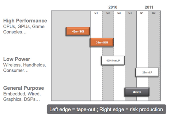
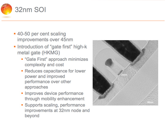
In the second half of 2010 Global will move one of its Dresden fabs to 32nm SOI production for AMD’s CPUs. I’m not expecting anything else to be made on this process other than AMD CPUs at this point.
We’ll see a “low power” 40/45nm process come out of Dresden near the end of 2010 as well. This will actually be for GF’s first non-AMD customer: STMicro.
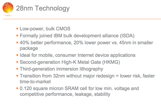
The real transition happens in 2011, when Global upgrades its older Dresden fab to support 28nm bulk silicon production. Globalfoundries views 28nm as the transition point for many potential customers. It’s not that there’s anything magical about 28nm, but many companies currently have designs for TSMC’s 40nm process and it makes little sense to redo them for manufacturing at Globalfoundries. At 28nm they can simply design for Globalfoundries’ process from the start.
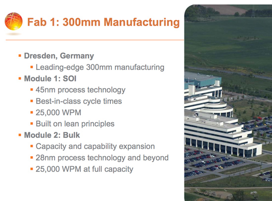
The fabs formerly known as Fab 30 and 36
Note that this 28nm process is a “half-node” (between 32nm and 22nm) and where I’m expecting to see ATI (and NVIDIA) GPUs made at Globalfoundries. The current 40nm products are being made at TSMC but it’s possible that we’ll see the next-generation pitched to GF. The first hybrid CPU/GPU from AMD will be built on GF’s 22nm SOI process in 2012.
Bulk vs. SOI
Back in 2001 AMD started to move to SOI (Silicon on Insulator) for its CPU manufacturing. The benefits of SOI were lower power and faster switching rates, although it came at a higher manufacturing cost. AMD will continue to use SOI for its high performance CPUs because their price can justify the additional manufacturing cost. More price sensitive markets don’t need the performance benefits of SOI and would rather not deal with the price penalties of it either; for those companies Globalfoundries needs to provide a bulk silicon process and in 2010, they will get just that.
Enabling SOI as well as bulk silicon manufacturing isn’t all that difficult but it does require some work. The first bulk process in Dresden will be a 40nm low power process out of Fab 1 Module 1. The first customer? Not AMD, but rather STMicro. These are the folks who used to make the old Kyro graphics cards, but obviously they’ll be making low power SoCs here instead.
In 2011 Global will offer a 28nm LP bulk process as well as a 28nm general purpose bulk process. The latter will be used for GPUs and other non-ultra-low-power devices.
Again, all of these plans involve AMD’s old fabs in Dresden, Germany (formerly Fab 36 and Fab 30, now Fab 1 Modules 1 and 2). Once 2012 rolls around, there will be a new player in town.


50 Comments
View All Comments
drwho9437 - Saturday, August 8, 2009 - link
I think Anand is correct that FABs are ridiculously expensive and that the volume leader has a major advantage. However, it remains to be seen if the spin off is a good move for AMD.The honest truth is that 15 nm is probably the end of the road for gate lengths. That is a few generations away. Lithography can improve all you want it to, but leakage and process variability become more and more important as you go down in size. At 10 nm cube of Silicon has about 100,000 atoms in it. Even at 10^20 /cm^3 doping levels you are talking about 100 atoms in the channel. That's 10% variability in doping... 32 28 22 18 end of the road my friends. Of traditional Silicon that is. There really isn't anything right now to easily replace it, its just so nice chemically...
People will say the end has been predicted forever, and then claim I am wrong (at least that is what normally happens when I say this). I may be wrong but that isn't why. The sun comes up every day but one day it won't. One day we will hit the physical limits of Silicon and from my point of view it will be the statistical that will certainly be a problem. I think you'll see problems at around 10-15 nm.
What is exciting it the idea that we will have to finally be more cleaver than drawing smaller lines in Si and think of something truly original to make progress...
But given that that original idea may either take time to materialize or that it might be expensive, I think you will see reliable Si for a LONG time at some dimension. 40 or 32 nm may be with us a for decades in many types of systems... Given this, the cost of upgrading FABs may stop because there will be no more upgrades. Then you ask do you want control over them or not... I can see arguments on both sides. Certainly in the near future AMD had no choice cash flow wise.
There are other ways to innovate other than die shrinks, and leaning on optics and chemistry. We shall see if we are cleaver enough.
cosminliteanu - Monday, August 3, 2009 - link
Thank you for this article :)zodiacfml - Sunday, August 2, 2009 - link
Thanks Anand! Some good posted comments too.toyotabedzrock - Saturday, August 1, 2009 - link
$88M / 1,400 Jobs = $62,875. So a lot of the jobs must be for not highly skilled people? I consider highly skilled to be worth $80-100K.Doesn't the US control how much of our most advanced tech is exported to certain countries? We only just recently allowed Intel to build a 65nm fab in China.
drwho9437 - Saturday, August 8, 2009 - link
Typical FAB worker would probably hold a BS in EE, Chem, Mat Sci, starts at about 42-50K when I graduated undergrad. Those 10K slots add up for the MS/PhD who run the line or whatever.mesiah - Thursday, July 30, 2009 - link
Great article! I love reading stuff like this. I am by far not an expert in the field, but it sounds like EUV could revolutionize the chip making process. Although it looks like it still has a significant number of hurdles to overcome, especially when it comes to WPH. Also an exciting prospect but many more years off is the current research with graphene. Its hard to imagine the processing power we will be able to harness in the near future. Alot of people take for granted the devices we use today. Things like iphones and netbooks were hardly dreamed of when I was a kid. Sure, we talked about seeing stuff like this 15 years ago, but I guess I never believed it would happen so fast.MODEL3 - Wednesday, July 29, 2009 - link
Great article.I just have some questions regarding fab companies such TSMC:
Until 180nm, we had a very good tempo for manufacturing proccess transitions.
Then suddenly, from 180nm to 90nm there was a very profound deceleration.
Then from 90nm to 40nm (and for the medium-term future) we have an increase of the tempo again.
Why they keep increasing the tempo?
You said that the R&D cost increased dramatically and that the Fab Start-up Cost increased dramatically also. (I am not arguing, after all I don't have a technological background)
So if for a company such TSMC, the cost has increased so much more in relation with the past then it should charge their customers per wafers (per size counted in) much more, right?
Then Why between 90nm and 55nm:
The die size per price range increased exponentially (I have done the calculations with Nvidia chips because the "die information" was more easily found on the net)
This is a fact.
Unless that your explanation is simply that Nvidia & ATI made way way more money back then, or that TSMC was robbing Nvidia/ATI back then, what is your explanation?
I mean that, yes it is easy to figure out that Nvidia & ATI made more money back then, but the financial data does not support such a huge difference.
My guess (out of the conspiracy book) is that already exists a valid successor of silicon based type methods and they just milking the current technology (for the next 5-10 years)
(I am not talking about technologies to scale down lithography, like alpha EUV, I am talking about THE next step to silicon based types)
In another subject you said:
Note that this 28nm process is a “half-node” (between 32nm and 22nm) and where I’m expecting to see ATI (and NVIDIA) GPUs made at Globalfoundries"
Why are you expecting 28nm to be that process?
Do you think that after 28nm the TSMC will skip 22nm (like they did with 45nm) and focus on 20nm (so the transition will take them more time), so GF will find an opportunity to offer something competitive?
drwho9437 - Saturday, August 8, 2009 - link
High K and SOI both expensive gave new breathing room. But they both are stop gap measures... Bigger problems to come. Expect 32 nm and the next node to go OK then bigger fish enter the picture.Also don't expect way higher frequencies. 2 GHz is pretty easy to design. I can do a PCB that is flat to 2 GHz in about an hour... Designing in the X band however is painful.
Still all sorts of interesting things going on outside Si, organics, molecular switches, terahertz, optics on chips, the return of magnetic. They are all pain in the butt compared to better lithography though :-)
Zagor Tenay - Wednesday, July 29, 2009 - link
Great article! It is so relieving to see that the whole semiconductor industry is not a captive at the hands of an ugly, greedy beast called INTEL.Zingam - Wednesday, July 29, 2009 - link
Don't forget that AMD owns the GF. If GF makes a profit. AMD gets revenues.I don't think that AMD does not have foundries anymore. They are just not attached to it. It isn't the same as NVIDIA - they do not possess anything like GF.