The SSD Anthology: Understanding SSDs and New Drives from OCZ
by Anand Lal Shimpi on March 18, 2009 12:00 AM EST- Posted in
- Storage
The Anatomy of an SSD
Let’s meet Mr. N-channel MOSFET again:
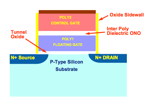
Say Hello
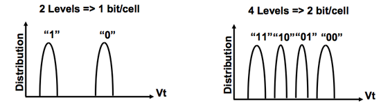
This is the building block of NAND-flash; one transistor is required per cell. A single NAND-flash cell can either store one or two bits of data. If it stores one, then it’s called a Single Level Cell (SLC) flash and if it stores two then it’s a Multi Level Cell (MLC) flash. Both are physically made the same way; in fact there’s nothing that separates MLC from SLC flash, it’s just a matter of how the data is stored in and read from the cell.
SLC flash (left) vs. MLC flash (right)
Flash is read from and written to in a guess-and-test fashion. You apply a voltage to the cell and check to see how it responds. You keep increasing the voltage until you get a result.
| SLC NAND flash | MLC NAND flash | |
| Random Read | 25 µs | 50 µs |
| Erase | 2ms per block | 2ms per block |
| Programming | 250 µs | 900 µs |
With four voltage levels to check, MLC flash takes around 3x longer to write to as SLC. On the flip side you get twice the capacity at the same cost. Because of this distinction, and the fact that even MLC flash is more than fast enough for a SSD, you’ll only see MLC used for desktop SSDs while SLC is used for enterprise level server SSDs.
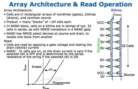
Cells are strung together in arrays as depicted in the image to the right
So a single cell stores either one or two bits of data, but where do we go from there? Groups of cells are organized into pages, the smallest structure that’s readable/writable in a SSD. Today 4KB pages are standard on SSDs.
Pages are grouped together into blocks; today it’s common to have 128 pages in a block (512KB in a block). A block is the smallest structure that can be erased in a NAND-flash device. So while you can read from and write to a page, you can only erase a block (128 pages at a time). This is where many of the SSD’s problems stem from, I’ll repeat this again later because it’s one of the most important parts of understanding SSDs.
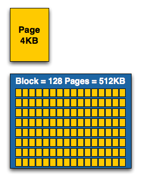
Arrays of cells are grouped into a page, arrays of pages are grouped into blocks
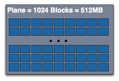
Blocks are then grouped into planes, and you’ll find multiple planes on a single NAND-flash die.
The combining doesn’t stop there; you can usually find either one, two or four die per package. While you’ll see a single NAND-flash IC, there may actually be two or four die in that package. You can also stack multiple ICs on top of each other to minimize board real estate usage.


250 Comments
View All Comments
matrixireland - Thursday, December 24, 2009 - link
hi would like to know what you pros think of the;Golden Leopard ASAX-ZIF1.8-SSD? what would you add to it?
And how would you rate it against other ssd?
Specifications:
product description
ASAX-ZIF1.8-SSD is a high-performance design solid state drive based on the high-end micro-control IC with flash memory storage medium integrated advantaged of high speed,convenient ,aseismatic,energy-saving etc.
specification
Model
Size
Interface
Material
ASAX-ZIF1.8-SSD
1.8inch 70×54×6mm
ZIF
Aluminum-magnesium alloy appearance ,drawbench and colorful oxidation surface,elegant temperament
performance
read speed:80- 96Mbytes/second write speed:50- 60Mbytes/second
support ATA-7 V3 PIO/multi word/ultra DMA MODES
Low power TFBGA,4 channel of flash controller,masked ROM and data SRAM
SAMSUNG flash keeps the data faster on reliability and endurance
Dynamic and static wear-leveling prolong NAND FLASH and SSD for longer life
8/16 bit BCH ECC data error correction ability effectively guarantee the data read security.
Design consideration
Capacity
16G/32G/64G/128G/256G
Average access time
<0.25MS
operating temperature
0-85°
power consumption
DC Input Voltage(3.3V or 5 V ± 10%)Read and write:135mA/194Ma wait:70mA
shock
1500G
Application
the Laptop, pc, server,workstation,portable media player,digital collection apparatus and any computer equipment which need consecutive read and write speed and high reliability storage.
jay401 - Wednesday, March 18, 2009 - link
yeah, he wants "more expensive than" or "too expensive for".Spoelie - Wednesday, March 18, 2009 - link
Second page as well:missing charts before and after this paragraph:
"The chart above shows how much faster these affordable MLC SSDs were than the fastest 3.5” hard drive in sequential transfers. But now look at random write performance:"
Spoelie - Wednesday, March 18, 2009 - link
chart 1 on page 2 now shows sequential read but the paragraph is changed to mention random read ;)page 21: As far as I know, this is THE one of THE only reviews
Some very surprising benchmark results for the ocz vertex, I thought the new firmware tanked sequential read speeds (to 80-90) based on the explanation beforehand, but not according to the actual graphs.
Spoelie - Wednesday, March 18, 2009 - link
third page, first table, first column: SSD and HDD entries are switchedmikaela - Tuesday, March 16, 2010 - link
yeah great info. also great resourceSpoelie - Wednesday, March 18, 2009 - link
page 19: I’d never reviewed it'd & -ed?
HolyFire - Wednesday, March 18, 2009 - link
"I'd never reviewed it" is correct. "I'd" here means "I had", it's Past Perfect tense.FishTankX - Wednesday, March 18, 2009 - link
That should have bolded "too"FishTankX - Wednesday, March 18, 2009 - link
Also, I think the velociraptor vs X-25 figures are swapped. 6 odd ms for the intel drive and 0.11ms for the velociraptor..