Nehalem Part 3: The Cache Debate, LGA-1156 and the 32nm Future
by Anand Lal Shimpi on November 19, 2008 8:00 PM EST- Posted in
- CPUs
Another Part? Oh there will be more
In an unexpected turn of events I found myself deep in conversation with many Intel engineers as well as Pat Gelsinger himself about the design choices made in Nehalem. At the same time, Intel just released its 2009 roadmap which outlined some of the lesser known details of the mainstream LGA-1156 Nehalem derivatives.
I hadn’t planned on my next Nehalem update being about caches and mainstream parts, but here we go. For further reading I'd suggest our first two Nehalem articles and the original Nehalem architecture piece.
Nehalem’s Cache: More Controversial Than You’d Think
I spoke with Ronak Singhal, Chief Architect on Nehalem, at Intel’s Core i7 launch event last week in San Francisco and I said to him: “I think you got the cache sizes wrong on Nehalem”. I must be losing my shyness.
He thought I was talking about the L3 cache and asked if I meant it needed to be bigger, and I clarified that I was talking about the anemic 256KB L2 per core.
We haven’t seen a high end Intel processor with only 256KB L2 per core since Willamette, the first Pentium 4. Since then Intel has been on a steady ramp upwards as far as cache sizes go. I made a graph of L2 cache size per core of all of the major high end Intel cores for the past decade:
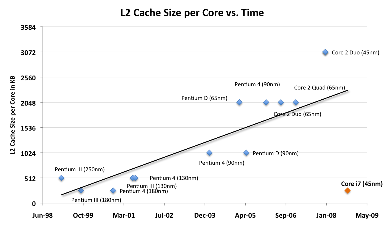
For the most part we’ve got a linear trend, there are a few outliers but you can see that earlier in 2008 you’d expect Intel CPUs to have around 2 - 3MB of L2 cache per core. Now look at the lower right of the chart, see the little orange outlier? Yeah, that’s the Core i7 with its 256KB L2 cache per core, it’s like 2002 - 2007 never happened.
If we look at total on-chip cache size however (L2 + L3), the situation is very different:
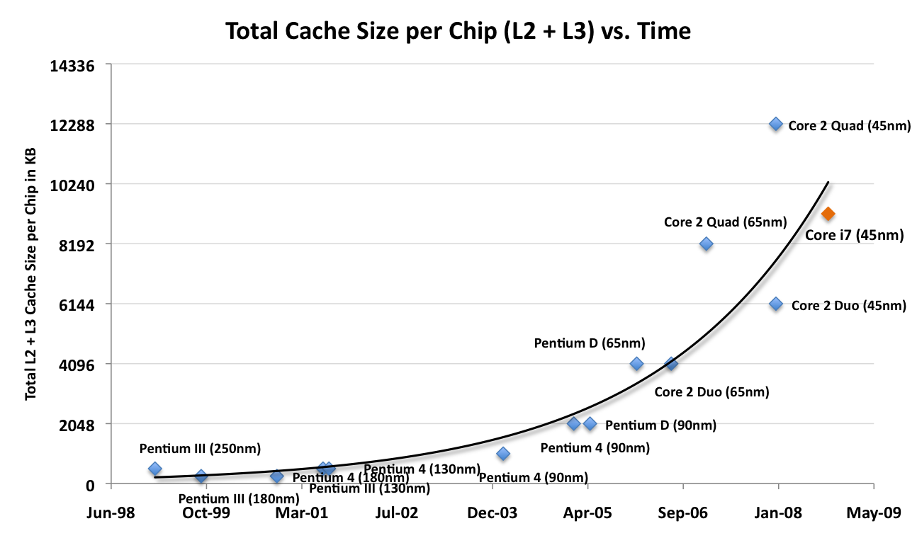
Now we’ve got an exponential growth of cache size, not linear, and all of the sudden the Core i7 conforms to societal norms. To understand why, we have to look at what happened around 2005 - 2006: Intel started shipping dual-core CPUs. As core count went up, so did the total amount of cache per chip. Dual core CPUs quickly started shipping with 2MB and 4MB of cache per chip and the outgoing 45nm quad-core Penryns had 12MB of L2 cache on a single package.
The move to multi-core chip designs meant that the focus was no longer on feeding the individual core, but making sure all of the cores on the chip were taken care of. It’s all so very socialist (oh no! ;) ).
Nehalem was designed to be a quad-core product, but also one that’s able to scale up to 8 cores and down to 2 cores. Intel believes in this multi-core future so designing for dual-core didn’t make sense as eventually dual-core will go away in desktops, a future that’s still a few years away but a course we’re on nonetheless.
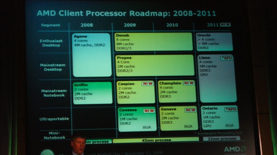
AMD's shift to an all quad-core client roadmap
Intel is pushing the shift to quad-core, much like AMD is. By 2010 all of AMD’s mainstream and enthusiast CPUs will be quad-core with the ultra low end being dual-core, a trend that will continue into 2011. The shift to quad-core makes sense, unfortunately today very few consumer applications benefit from four cores. I hate to keep re-using this same table but it most definitely applies here:
Back when AMD introduced its triple-core Phenom parts I put together a little table illustrating the speedup you get from one, two and four cores in SYSMark 2007:
| SYSMark 2007 Overall | E-Learning | Video Creation | Productivity | 3D | |
| Intel Celeron 420 (1 core, 512KB, 1.6GHz) | 55 | 52 | 55 | 54 | 58 |
| Intel Celeron E1200 (2 cores, 512KB, 1.6GHz) | 76 | 68 | 91 | 70 | 78 |
| % Increase from 1 to 2 cores | 38% | 31% | 65% | 30% | 34% |
| Intel Core 2 Duo E6750 (2 cores, 4MB, 2.66GHz) | 138 | 147 | 141 | 120 | 145 |
| Intel Core 2 Quad Q6700 (4 cores, 8MB, 2.66GHz) | 150 | 145 | 177 | 121 | 163 |
| % Increase from 2 to 4 cores | 8.7% | 0% | 26% | 1% | 12% |
Not only are four cores unnecessary for most consumers today, but optimizing a design for four cores by opting for very small, low latency L2 caches and a large, higher latency L3 cache for the chip isn’t going to yield the best desktop performance.
A Nehalem optimized for two cores would have a large L2 cache similar to what we saw happening on the first graph, but one optimized for four or more cores would look like what the Core i7 ended up being. What’s impressive is that Intel, in optimizing for a quad-core design, was still able to ensure that performance either didn’t change at all or improved in applications that aren’t well threaded.
Apparently the L2 cache size was and still is a controversial issue within Intel, many engineers still feel like it is too small for current workloads. The problem with making it larger is not just one of die size, but also one of latency. Intel managed to get Nehalem’s L2 cache down to 10 cycles, the next bump in L2 size would add another 1 - 2 cycles to its latency. At 512KB per core, 20% longer to access the cache was simply unacceptable to the designers.
In fact, going forward there’s no guarantee that the L2 caches will see growth in size, but the focus instead may be on making the L3 cache faster. Right now the 8MB L3 cache takes around 41 cycles to access, but there’s clearly room for improvement - getting a 30 cycle L3 should be within the realm of possibility. I pushed Ronak for more details on how Intel would achieve a lower latency L3, but the best I got was “microarchitectural tweaks”.
As I mentioned before, Ronak wanted the L3 to be bigger on Nehalem; at 8MB that’s only 2MB per core and merely sufficient in his eyes. There are two 32nm products due out in the next 2 years, I suspect that at least one of them will have an even larger L3 to continue the exponential trend I showed in the second chart above.
Could the L2 be larger? Sure. But Ronak and his team ultimately felt that the tradeoff between size/latency was necessary for what Intel’s targets were with Nehalem. And given its 0 - 60% performance increase, clock for clock, over Penryn - I can’t really argue.


33 Comments
View All Comments
IntelUser2000 - Saturday, November 22, 2008 - link
To: ltcommanderdataActually you can't compare to Dothan. You have to compare to Conroe/Penryn. Conroe's L2 latency is at 14 cycles. I think it went up to make up for the complexity of the core(which is more than Dothan). Nehalem makes it even more complex.
The reason individual transistors can run at 200GHz+ within certain research labs but nowhere near with a commercial chip is they have to synchronize every part of the chip with the clock.
The CPU designers seem to take some chances when making a chip. Likely that's the reason for the delays for certain products as if you make a wrong decision then the prototypes might not come up as you wanted and you gotta make up for it.
That's probably the reason that Conroe didn't come with SMT as the Israeli team managing the chip wasn't experienced as the team that made the P4. They probably could have but risking it would not have been a good idea.
The Israeli team clings on proven technologies while the Hillsbro team makes up more radical ones, like Trace Cache, Out of Order, SMT, etc.
JonnyDough - Friday, November 21, 2008 - link
It should be exactly like Penryn. Die shrink = less heat = higher clocks = performance increase.ltcommanderdata - Friday, November 21, 2008 - link
The point is that Penryn was not just a dumb shrink of Conroe with added cache as Presler was of Smithfield. Penryn wasn't a major redesign, but it did have architectural tweaks over Conroe including speeding up how the execution units divide numbers and execute shuffles. The FSB was also reworked to allow half multipliers while lower power states were added in mobile versions. VT support was enhanced and of course SSE4.1 was added.I believe clock-for-clock Penryn is on average 5% faster than Conroe while the difference can be substantially higher for SSE4.1 optimized apps. When I say I hope Westmere is more like Penryn, I'm hoping for similar tweaks to be made to increase performance clock-for-clock, rather than just relying on 32nm to increase clock speeds. I don't believe Intel is releasing another SSE instruction set before AVX in Sandy Bridge, so I guess they'll have to dig deeper for a performance boost.
VaultDweller - Thursday, November 20, 2008 - link
"We’re finally getting wind of X58 motherboards at well below $300"Oh, please do share! This is what I'm interested in. Without this I would not even consider touching Nehalem with a ten foot pole.
In the past I brushed off X38 and X48 completely, as it was so hard to find reasonable motherboards based on these chipsets. X58 is shaping up to be the same.
The problem is that when I found X38 to be too expensive, I was able to find my peace with a P35 board (a P5K Premium). If I had building a system when X48 was hot off the press, I could find comfort knowing that P45 was right around the corner. There is no such comfort with Nehalem - the only lower-priced chip platform on the radar is based on a different socket, like S754 all over again.
I don't want to cripple or limit the options for my next system build by going with LGA1156, but I don't want to pay $300-450 for a motherboard either.
heavyglow - Thursday, November 20, 2008 - link
this is exactly what im thinking. im concerned that intel will abandon LGA1156 and ill be left with nothing.3DoubleD - Thursday, November 20, 2008 - link
I can think of the reverse scenario where AMD abandoned the 940 platform and released all FX processors on 939. Neither option is safe, just pick one you don't mind sticking with if you have to.Kiijibari - Thursday, November 20, 2008 - link
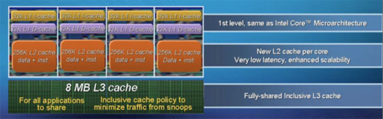
It's so small because Nehalem is a 100% Server design.Because of this Intel went ahead with the inclusive cache design. It comes in quite handy in MP systems, if you just have to probe one L3 only instead of 4 L1/L2 caches.
But there is one drawback, bigger L2 kills the benefit of the L3 size.
Neglecting the L1 Caches, Nehalem has an effective L3 size of 7 MB, as 4x256kb are just copied data from the L2.
Now imagine what would happen if intel would double the L2. Effective L3 cache size would have shrunk to 6MB, 2 MB waste .. that a lot of transistors.
To make L2 problems worse, Intel reintroduced Hyperthreading. Great technique, no doubt, but now we even have 2 threads struggling for the tiny, little 256kb cache.
I guess all the decisions pay off in a server environment, but to state that intel designed the small size L2 Caches because of the latency only is just a fine excuse for all the wanna-be gamers, who once heard that CL3 memory is better than CL5.
cheers
Kiiji
plonk420 - Thursday, November 20, 2008 - link
If 8core i7s will work on x58, i'll likely bite sooner rather than doing a "wait and see."does this seem highly likely? or is it anyone's guess?
Casper42 - Thursday, November 20, 2008 - link
Speaking of which, I ran across this today on accident:http://www.ecs.com.tw/ECSWebSite/Downloads/Product...">http://www.ecs.com.tw/ECSWebSite/Downlo...ilName=M...
The ECS X58B-A
Contains:
6 DDR3 Slots
2 x16 Slots
1 x4 Slot
2 x1 Slots
1 PCI Slot
The Manual makes mention of SLI as well which was surprising to me.
I can see that a machine with this ECS Board, a 920 proc and 2 x 9800GTX+ cards (Currently going for around $150 each) and you could have a pretty potent little machine for around $1000
iwodo - Thursday, November 20, 2008 - link
So we wont see new Mobile Part till 2010 ?That doesn't sound right to me at all. If that is the case then the rumours about it being a 32nm part may be right.
However, the idea Intel not updating their Mobile Part for 18 months doesn't sound right to me at all.