The Dark Knight: Intel's Core i7
by Anand Lal Shimpi & Gary Key on November 3, 2008 12:00 AM EST- Posted in
- CPUs
Our First X58 Motherboard Preview: The ASUS Rampage II Extreme
We utilized the ASUS Rampage II Extreme motherboard for our overclocking and memory tests in today’s article. We will take a detailed look at this board and others from MSI, Gigabyte, ASUS again, and Intel in few days. Boards from these particular manufacturers will be available shortly and our review samples now feature retail production kits, not engineering or early production samples.
All of the boards have performed very well so far, but we have been on the BIOS of the day merry-go-round for the last week or so. However, it appears the current BIOS releases are finally to the point of being acceptable for public release, not exactly perfect yet, but a multitude of problems have been addressed over the past few weeks.
That said, this particular board is designed for a very niche market and will see limited production numbers. The mainstream enthusiast board from ASUS will be the P6T Deluxe board, a board that we actually prefer in most cases. This ROG board will be ASUS’s primary weapon in the ultra high-end market against some stiff competition from the Gigabyte EX58 Extreme board. Pricing is not set yet, but we expect it to be around $400. ASUS includes an extensive accessory kit that features their external LCD poster.
As expected with an Republic of Gamers motherboard, the BIOS options are extensive and well laid out. Of note, the QPI/DRAM Core Voltage is not the DRAM voltage setting. We think it should actually be called QPI/IMC or just Uncore voltage. In fact, as we discussed earlier, this voltage setting could potentially be more damaging to the CPU than the 1.65V recommendation on DRAM. Otherwise, the BIOS is straight forward and allows for a myriad of tuning options. We were able to easily get our i7 965 samples up to 4.2GHz on air (not the retail cooler), water, and our CoolIT Systems Freezone Elite. Our i7 920 samples reached about 3.8GHz, although we think there is a possibility for stable 4GHz operation with them.
The Big Picture
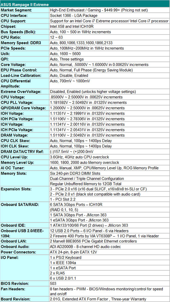
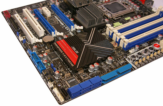
This board compares well to the previous Maximus Formula II and Rampage Extreme boards. We have the return of an eight-layer board dressed out in our favorite black, silver, and Ferrari red primary color scheme. The memory and peripheral slots return in a blue and white motif with the first PCI Express x1 slot that usually houses the SupremeFX X-FI audio card sporting black.
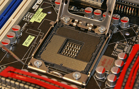
Due to the new LGA 1333 (Socket B1) design that is larger than the current LGA 775 along with six DIMM slots, the area around the CPU is crowded, resulting in a creative layout design that manages to squeeze all the options in a slightly extended ATX format. However, the layout just does not look as clean as previous ROG offerings to us although it is still aesthetically pleasing. ASUS throws in eight fan headers that can be controlled and monitored in the BIOS or via a Windows utility program.
Around the Board
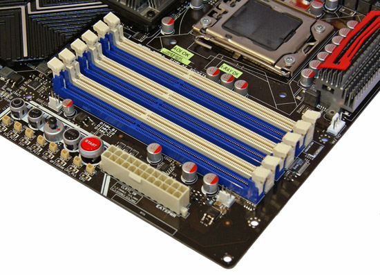
Six DDR3 DIMM slots are included for tri-channel goodness. Performance and compatibility continues to be better when utilizing the blue slots. The memory sub-system receives a three-phase power delivery system.
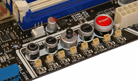
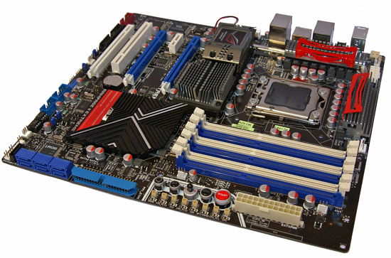
The TweakIT toggle and power/reset switches carry over from the Rampage Extreme board. This system lets you overclock on the fly from within Windows or even during applications when the CPU is loaded. Eight different solder points and pin-outs allow multimeter readings of DIMM, ICH, ICH PCIe, IOH, QPI, CPU PLL, and Core voltages.
The ICH10R Southbridge is utilized and provides the six SATA ports (dark blue) along with RAID 0,1,5,10. ASUS reverted to the JMicron JMB363 for an extra SATA port (black), an eSATA port on the IO panel and IDE duties. The iROG chipset returns and offers the same features as before, on-board LED control, time keep function, BIOS flashback, additional voltage controls, and a temperature based protection scheme if you enable it.
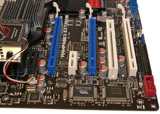
ASUS includes two PCI Express 2.0 x1 slots, three x16 PCIe 2.0 slots (dual x16 or tri x16/x8/x8), and a lonely PCI slot. Tri-Crossfire and SLI support is included, we just need better drivers from AMD/NVIDIA to recognize the graphics potential of this platform. If you utilize double slot GPU cards, the second PCIe x1 slot and the PCI slot will be physically unavailable with a CF or SLI setup.
The black PCIe x1 slot doubles as the HD Audio slot that features the ADI SoundMAX 2000B chipset with support for Creative X-FI 4.0 routines via a software implementation. This is the last hurrah for the ADI chipset as they have exited the on-board audio business but will continue to provide support into the near future.
Below the ROG silkscreen is the VTT CPU Power Card. The second heatsink is for the X58 chipset and works quite well in early testing. However, if you are running a CF or SLI setup and need the first PCIe x1 slot for audio or other purposes, you are out of luck as the last set of fins on the heatsink blocks full-length cards. We hope that ASUS will address this before commencing retail production.
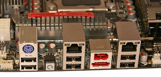
The IO panel is standard and almost legacy free. The PS/2 keyboard port is a nod to the overclocking crowd as is the clear CMOS switch. Six USB 2.0 ports are available along with six more via headers on the motherboard. An IEEE 1394a port courtesy of the fast VIA VT8308P chipset and the eSATA port via a JMicron 363 are included along with dual RJ-45 ports sporting the Marvell 88E8056-NNC1 controller chips that offer teaming capability.
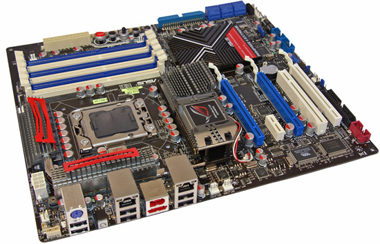
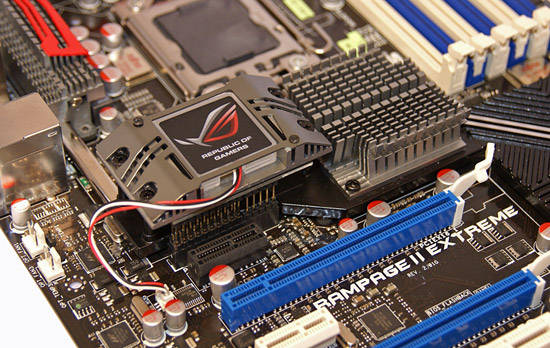
CPU Real Estate
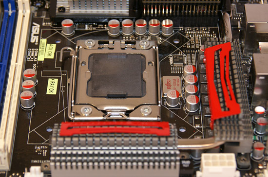
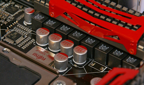
The CPU socket area is crowded but manageable for most cooling setups. ASUS utilizes their “16-phase” power delivery system along with a 3-phase system for the Northbridge. The EPU2 design allows switching between four or sixteen phases to save energy although we think anyone with this board is probably not concerned with it. The board utilizes a combination of Fujitsu ML and Solid Aluminum capacitors.
That concludes our quick overview of the ASUS Rampage II Extreme board. We will be back shortly with full reviews of several X58 boards.


73 Comments
View All Comments
Kaleid - Monday, November 3, 2008 - link
http://www.guru3d.com/news/intel-core-i7-multigpu-...">http://www.guru3d.com/news/intel-core-i...and-cros...bill3 - Monday, November 3, 2008 - link
Umm, seems the guru3d gains are probably explained by them using a dual core core2dou versus quad core i7...Quad core's run multi-gpu quiet a bit better I believe.tynopik - Monday, November 3, 2008 - link
what about those multi-threading tests you used to run with 20 tabs open in firefox while running av scan while compressing some files while converting something else while etc etc?this might be more important for daily performance than the standard desktop benchmarks
D3SI - Monday, November 3, 2008 - link
So the low end i7s are OC'able?
what the hell is toms hardware talking about lol
conquerist - Monday, November 3, 2008 - link
Concerning x264, Nehalem-specific improvements are coming as soon as the developers are free from their NDA.See http://x264dev.multimedia.cx/?p=40">http://x264dev.multimedia.cx/?p=40.
Spectator - Monday, November 3, 2008 - link
can they do some CUDA optimizations?. im guessing that video hardware has more processors than quad core intel :PIf all this i7 is new news and does stuff xx faster with 4 core's. how does 100+ core video hardware compare?.
Yes im messing but giant Intel want $1k for best i7 cpu. when likes of nvid make bigger transistor count silicon using a lesser process and others manufacture rest of vid card for $400-500 ?
Where is the Value for money in that. Chukkle.
gramboh - Monday, November 3, 2008 - link
The x264 team has specifically said they will not be working on CUDA development as it is too time intensive to basically start over from scratch in a more complex development environment.npp - Monday, November 3, 2008 - link
CUDA Optimizations? I bet you don't understand completely what you're talking about. You can't just optimize a piece of software for CUDA, you MUST write it from scratch for CUDA. That's the reason why you don't see too much software for nVidia GPUs, even though the CUDA concept was introduced at least two years ago. You have the BadaBOOM stuff, but it's far for mature, and the reason is that writing a sensible application for CUDA isn't exactly an easy task. Take your time to look at how it works and you'll understand why.You can't compare the 100+ cores of your typical GPU with a quad core directly, they are fundamentaly different in nature, with your GPU "cores" being rather limited in functionality. GPGPU is a nice hype, but you simply can't offload everything on a GPU.
As a side note, top-notch hardware always carries price premium, and Intel has had this tradition with high-end CPUs for quite a while now. There are plenty of people who need absolutely the fastest harware around and won't hesitate paying it.
Spectator - Monday, November 3, 2008 - link
Some of us want more info.A) How does the integrated Thermal sensor work with -50+c temps.
B) Can you Circumvent the 130W max load sensor
C) what are all those connection points on the top of the processor for?.
lol. Where do i put the 2B pencil to. to join that sht up so i dont have to worry about multiply settings or temp sensors or wattage sensors.
Hey dont shoot the messenger. but those top side chip contacts seem very curious and obviously must serve a purpose :P
Spectator - Monday, November 3, 2008 - link
Wait NO. i have thought about it..The contacts on top side could be for programming the chips default settings.
You know it makes sence.Perhaps its adjustable sram style, rather than burning connections.
yes some technical peeps can look at that. but still I want the fame for suggesting it first. lmao.
Have fun. but that does seem logical to build in some scope for alteration. alot easier to manufacture 1 solid item then mod your stock to suit market when you feel its neccessary.
Spectator.