NVIDIA's 1.4 Billion Transistor GPU: GT200 Arrives as the GeForce GTX 280 & 260
by Anand Lal Shimpi & Derek Wilson on June 16, 2008 9:00 AM EST- Posted in
- GPUs
Tweaks and Enahancements in GT200
NVIDIA provided us with a list, other than the obvious addition of units and major enhancements in features and technology, of adjustments made from G80 to GT200. These less obvious changes are part of what makes this second generation Tesla architecture a well evolved G80. First up, here's a quick look at percent increases from G80 to GT200.
| NVIDIA Architecture Comparison | 8800 GTX | GTX 280 | % Increase |
| Cores | 128 | 240 | 87.5% |
| Texture | 64t/clk | 80t/clk | 25% |
| ROP Blend | 12p / clk | 32p / clk | 167% |
| Max Precision | fp32 | fp64 | |
| GFLOPs | 518 | 933 | 80% |
| FB Bandwidth | 86 GB/s | 142 GB/s | 65% |
| Texture Fill Rate | 37 GT/s | 48 GT/s | 29.7% |
| ROP Blend Rate | 7 GBL/s | 19 GBLs | 171% |
| PCI Express Bandwidth | 6.4 GB/s | 12.8GB/s | 100% |
| Video Decode | VP1 | VP2 |
Communication between the driver and the front-end hardware has been enhanced through changes to the communications protocol. These changes were designed to help facilitate more efficient data movement between the driver and the hardware. On G80/G92, the front-end could end up in contention with the "data assembler" (input assembler) when performing indexed primitive fetches and forced the hardware to run at less than full speed. This has been fixed with GT200 through some optimizations to the memory crossbar between the assembler and the frame buffer.
The post-transform cache size has been increased. This cache is used to hold transformed vertex and geometry data that is ready for the viewport clip/cull stage, and increasing the size of it has resulted in faster communication and fewer pipeline stalls. Apparently setup rates are similar to G80 at up to one primative per clock, but feeding the setup engine is more efficient with a larger cache.
Z-Cull performance has been improved, while Early-Z rejection rates have increased due to the addition of more ROPs. Per ROP, GT200 can eliminate 32 pixles (or up to 256 samples with 8xAA) per clock.
The most vague improvement we have on the list is this one: "significant micro-architectural improvements in register allocation, instruction scheduling, and instruction issue." These are apparently the improvements that have enabled better "dual-issue" on GT200, but that's still rather vague as to what is actually different. It is mentioned that scheduling between the texture units and SMs within a TPC has also been improved. Again, more detail would be appreciated, but it is at least worth noting that some work went into that area.
Register Files? Double Em!
Each of those itty-bitty SPs is a single-core microprocessor, and as such it has its own register file. As you may remember from our CPU architecture articles, registers are storage areas used to directly feed execution units in a CPU core. A processor's register file is its collection of registers and although we don't know the exact number that were in G80's SPs, we do know that the number has been doubled for GT200.
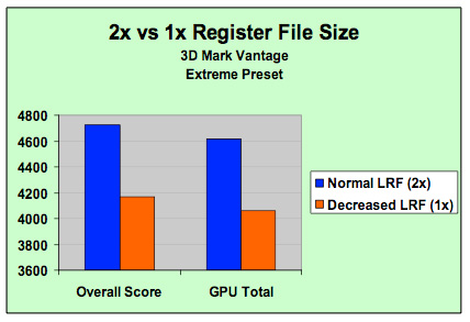
NVIDIA's own data shows a greater than 10% increase in performance due to the larger register file size (source: NVIDIA)
If NVIDIA is betting that games are going to continue to get more compute intensive, then register file usage should increase as well. More computations means more registers in use, which in turn means that there's a greater likelihood of running out of registers. If a processor runs out of registers, it needs to start swapping data out to much slower memory and performance suffers tremendously.
If you haven't gotten the impression that NVIDIA's GT200 is a compute workhorse, doubling the size of the register file per SP (multiply that by 240 SPs in the chip) should help drive the idea home.
Double the Precision, 1/8th the Performance
Another major feature of the GT200 GPU and cards based on it is support for hardware double precision floating point operations. Double precision FP operations are 64-bits wide vs. 32-bit for single precision FP operations.
Now the 240 SPs in GT200 are single-precision only, they simply can't accept 64-bit operations at all. In order to add hardware level double precision NVIDIA actually includes one double precision unit per shading multiprocessor, for a total of 30 double precision units across the entire chip.
The ratio of double precision to single precision hardware in GT200 is ridiculously low, to the point that it's mostly useless for graphics rasterization. It is however, useful for scientific computing and other GPGPU applications.
It's unlikely that 3D games will make use of double precision FP extensively, especially given that 8-bit integer and 16-bit floating point are still used in many shader programs today. If anything, we'll see the use of DP FP operations in geometry and vertex operations first, before we ever need that sort of precision for color - much like how the transition to single precision FP started first in vertex shaders before eventually gaining support throughout the 3D pipeline.
Geometry Wars
ATI's R600 is alright at geometry shading. So is RV670. G80 didn't really keep up in this area. Of course, games haven't really made extensive use of geometry shaders because neither AMD nor NVIDIA offered compelling performance and other techniques made more efficient use of the hardware. This has worked out well for NVIDIA so far, but they couldn't ignore the issue forever.
GT200 has enhanced geometry shading support over G80 and is now on par with what we wish we had seen last year. We can't fault NVIDIA too much as with such divergent new features they had to try and predict the usage models that developers might be interested in years in advance. Now that we are here and can see what developers want to do with geometry shading, it makes sense to enhance the hardware in ways that support these efforts.
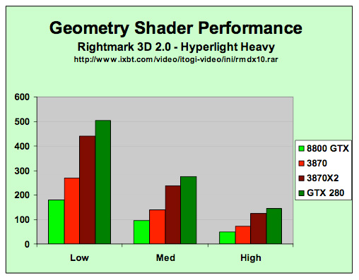
GT200 has significantly improved geometry shader performance compared to G80 (source: NVIDIA)
Generation of vertex data is a particularly weak part of NVIDIA's G80, so GT200 is capable of streaming out 6x the data of G80. Of course there are the scheduling enhancements that affect everything, but it is unclear as to whether NVIDIA did anything beyond increasing the size of their internal output buffers by 6x in order to enhance their geometry shading capability. Certainly this was lacking previously, but hopefully this will make heavy use of the geometry shader something developers are both interested in and can take advantage of.


108 Comments
View All Comments
epobirs - Monday, June 16, 2008 - link
There is an important precedent that gives Nvidia good reason to not rush to a new smaller process level. Recall when ATI first became a serious player in gaming GPUs with the 9700. It was for its time a big chip pushing the limits of the process level, while Nvidia at the time was concentrating on bleeding edge technology. Nvidia's chips got stomped by ATI's in that generation, in large part because the ATI chip had far better optimization of its transistors.anartik - Monday, June 16, 2008 - link
We can agree the pricing sucks. But the point that seems to be missing is that Nvidia promised a 50% performance improvement and they delivered. The 280 delivers 45FPS vs 32FPS for the 9800GT in Assassins creed. Thats just shy of 50% (48FPS) which is a huge performance increase compared to what we have been getting the past couple years for a new card. Slap 2x280 on a card and it vaporizes the 9800 GX2 or any SLI/Xfire solution. The 9800 GX2 scales ~63% over the 9800GTX. So if you do that for a 280GX2 (or SLI) you get roughly 73 frames per second. Plus the new cards have more memory to deal with bandwidth and large textures vs the nuetered 512 on the 96/9800's and 8800GT... the reason I have held onto my 8800 GTX with 768mb. Granted I won't be rushing out and buying one tomorrow but the 280 is the fastest GPU and a x2 will be faster than any other x2 card. It's a little rediculous to think the single 280 sucks becuase it's not faster than multiple GPU's like the 9800 GX2 (although when memory counts it is).araczynski - Monday, June 16, 2008 - link
this is all they could spit out? all that noise and all those transistors and it gets its ass handed to it by the gx2 more often than not?talk about fizzle, perhaps at best it'll lower the price of the gx2 a bit.
not to mention no built in hdmi, good lord, they must've had two seperate teams working on the gtx and gx2 at the same time and just wanted to see what they could come up with separately.
Ananke - Monday, June 16, 2008 - link
I don't think many people at this forum tread understand that nVidia target is the supercomputer market. I was totally impressed from one post a month ago, where a software engineer managed to put and use 3 SLI system for magnetoresonance rendering. Nvidia and AMD /that's why they acquired ATI/ have already significant experience in multiprocessor and parallel calculation. nVidia is ahead though, since they have CUDA becoming more popular for complex calculation. A year ago Intel realized parallel processing from Sun is their biggest danger, now nVidia and Ati come too. Imagine, supercomputers build with thousands of G200 chips, and only some Intels used for mapping, instead of thousands of Xeons. nVidia thinks way more ahead just for the mere visual/gaming market. I am very very impressed, and very eager to see what ATI can do. Also, I hope Ati and Havoc will be able to offer competition to CUDA, or uniformity? Anyway, from a scientific point of view, recent developments in the graphic market make foundamental science more affordable than anytime before.Reflex - Monday, June 16, 2008 - link
Anand/Derek -I am not sure why you are comparing this chip to a Penryn or other general purpose CPU as the comparisons are meaningless. GPU's are designed very differently than CPU's, namely a high level descriptor language is used and the design is then created by a program, which is then hand tweaked by engineers. By contrast, a CPU may use a high level language, but the actual design is almost entirely done by hand, with large teams working on each sub component and literally years of tweaking. It takes Intel between five and ten years to bring a design to market, which is why there is such a push by them to keep adjusting the design and optimizing it to stretch its usefulness out as long as possible to maximize the initial investment. This simply does not happen with a GPU.
GPU's are designed to last 18-24 months as a competitive solution. nVidia and Ati cannot afford to spend even five years designing them. As a result the level of hand optimization is greatly reduced, and inefficiencies with transistors are tolerated. Typically they are produced on equipment that is already paid for by the previous, more optimized products, or contracted out to third parties(TSMC). Since the products are sold for a premium, the wasted die space is not very relevant. It is a diametrically opposed process to what you see with CPU development.
Despite how impressive it may seem to go on about 1.4 billion transisters, truthfully a modern CPU does more with far less than a modern GPU, and honestly neither nVidia nor Ati are in the same league as Intel and AMD, neither at the engineering level nor when comparing the products they put out. To an Intel engineer, this GPU is at least four times larger than it needs to be to get the performance you get out of it.
The maturation of the industry, either due to reaching a point where GPU's can do 90% of what anyone needs, or simply because power budgets get more restrictive, will come when the level of optimization required for a CPU is required for a GPU, and product cycles stretch out to 3-5 years. Then you will have a more direct comparison between the two, since the design parameters will be much more similiar.
I am not knocking nV here, btw, I'm simply calling into question why one would even compare a Penryn to a GPU, it makes no sense at all when they were designed from the ground up for different purposes, lifespans and with different transister budgets.
7Enigma - Tuesday, June 17, 2008 - link
I think what this shows is there a brute force way of doing something that while not necessarily pretty can get you to a goal. Yes compared to Intel's latest and greatest it is a grotesque abomination of wasted energy/transistors/die size, but the bottom line is it is pretty darn impressive from a CPU/GPU standpoint.I think many of us long for the days of more than 2 major competetors for each race (CPU/GPU). We've been stuck in a rut with ATI and Nvidia, AMD and Intel. Yes you have some niche products by other companies, and budget pieces being made by a host of has-beens, but really tier 1 stuff is just not being fought over by more than 2 companies.
What I want to see (complete dreamland here) is a start up from some very savvy disgruntled employees of say AMD/ATI, Intel, IBM, etc. (and don't forget possibly the most important segment, the marketing team) with some clout and a LOT of dough to say, "Screw this, we're going balls to the wall and throw the kitchen sink at the market."
I mean let's be honest here, what's another 100 watts or a billion transistors anymore? I can guarantee you every geek out there would shell out more money for a product that devestates the current competition. I don't care if it's not as frugal with the power, or as small, or as pretty, I want the speed man, gimme the speed!
Anand Lal Shimpi - Monday, June 16, 2008 - link
While I'd normally agree with you, GPUs have been getting pretty complex to design. Much of the shader multiprocessors in G80 and GT200 were designed by hand, and remember that G80 (the original predecessor to GT200) was in development for four years before its launch.The transistor comparison is a valid one, while Penryn is a very impressive design, it is so for different reasons than GT200. The size of GT200 also helps illustrate fundamental differences in approach to CPU vs. GPU design and really highlights why Intel is building Larrabee.
-A
crimson117 - Monday, June 16, 2008 - link
Because to non-engineers, they're two silicon computer chips, and 1.4 billion of anything is a lot!It also helps me to visually understand why this thing gets so hot, since it's got so much more surface area packed with transistors.
You're right that CPUs and GPUs are designed for different tasks and shouldn't be considered pure apples to apples, but then you go against your own advice and start saying how CPUs are so much more advanced, and how Intel engineers could do that in 1/4 the size of a chip. So which is it - should they be compared, or should they not be compared?
And the authors did mention how simple it could be for either company to slap the other type of chip right in with their usual type; make a Intel CPU with added GPU capabilities, or make a nVidia GPU with CPU capabilities. So there's another point where they recognize the differences but do try to illustrate the sameness.
So I'm not really sure your criticisms hold water.
Reflex - Monday, June 16, 2008 - link
You are looking for contradictions where there are none. A chip is a chip, but that does not mean that they are all designed with the same goals, budgets and time constraints. *IF* Intel devoted the resources to a GPU that they devote to a CPU, yes they could produce a product like this in a fraction of the transisters. That said, the product would take 5-10 years to design, would cost hundreds of millions of dollars to develop, and would need a lifespan of at least 5 years in the market to be worth the effort. Obviously this is not a reasonable approach in a market with such fast product turnover.My post was not an attempt to diss nV or this product, it was pointing out that the comparison of a GPU to a CPU is inane as they have completely different design constraints. You may as well compare a CPU to cache memory, or RAM or a sound processor. All have transisters, right?
It especially bothered me when they implied that nVidia has the transister budget to toss a general purpose CPU on the die. The fact is that they may have the transister budget, but they do not have the time or money available to do so, and the product would be obsolete before it ever hit the market as a result of such an attempt. It would be marrying two completely different design philosophies, and this is why the combined CPU/GPU products that are upcoming are not likely to be the strongest performers.
paydirt - Monday, June 16, 2008 - link
You all seem to be assuming that GPUs will only be used for games. If that's all you care about, then why do you whine when a GPU is made to perform well as a number cruncher (for science, for modeling/simulations)?It's the best single GPU gaming card.
It's the best widely (?) available GPU number cruncher.
For a whole system gaming GPU solution, it isn't the most cost effective.
If you're all into numbers, then why are you assigning emotions to it. It simply is what it is.