DFI X48 LT T2R: Floats like a Butterfly…
by Rajinder Gill on April 28, 2008 4:00 AM EST- Posted in
- Motherboards
Toe to Toe with the BIOS (cont'd)
 |
 |
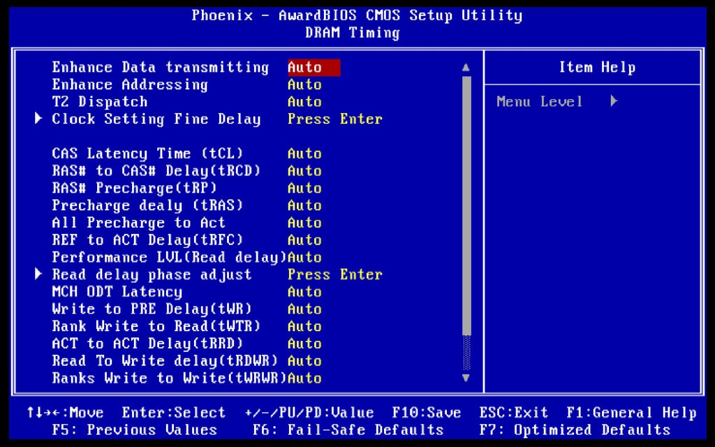
Regardless of individual memory timing preferences, to obtain best RAM/chipset latency performance we recommend that the following BIOS functions be set as follows for Micron D9-based RAM modules.
Enhance Data Transmitting: FAST
FAST MODE: Gives latency and bandwidth improvements over the "Normal" setting without overly affecting memory stability or FSB overclocking potential throughout the frequency ranges of interest for everyday use.
TURBO MODE: More suited to benchmarking runs. This is a very aggressive setting, further improving latencies past "Fast" mode. Using "Turbo" mode may require that the "CH1CH2 Common CLK Crossing Setting" be set to "Nominal" rather than "More Aggressive". VNB requirements are 1.7V and upwards, hence this should be used strictly for short-term benchmarking.
Enhance Addressing: FAST
This brings additional gains of latency and bandwidth used in combination with the above setting for best overall system performance. Again, the stability/voltage requirement hit is only minor for normal PC use. Although the BIOS defaults to Normal mode for both settings, there is no reason to veer away from setting FAST for both functions, provided you're using reasonable memory.
T2 Dispatch: Set this to Disabled, as it gives more overall stability when memory is clocked to high speeds.
 |
Channel 1 CLK Crossing Setting: More Aggressive
Channel 2 CLK Crossing Setting: More Aggressive
CH1CH2 Common CLK Crossing Setting: More Aggressive
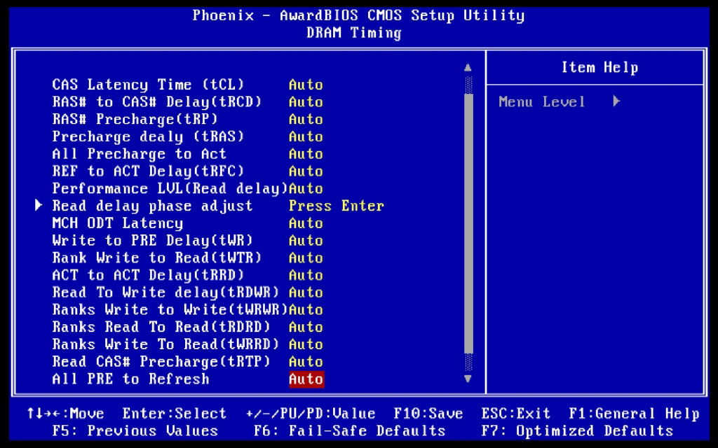
24/7 systems using Micron D9GMH-based modules will certainly want to take advantage of using all three of these settings in unison for a latency and bandwidth boost. We have found these three functions set to "More Aggressive" do not hinder the boards FSB progress excessively. Other RAM modules may not fare as well, unfortunately. Given the choice between a hike in tRD (performance level) or setting the clock crossing settings less aggressively, always strive to maintain the lowest tRD possible. Taking a hit in the clock crossing setting is not as drastic as additional clock delays to the tRD transfer cycle.
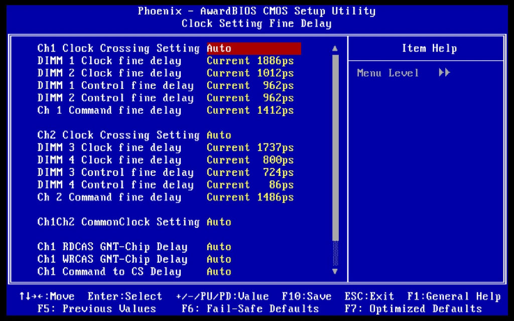
Clock Fine Delays: For both channels, the BIOS adjusts these values automatically when set to CURRENT mode. The scale runs in picoseconds of delay for each setting/channel. Generally, engineers do a very good job of ensuring PCB trace lengths to each DIMM slot on the motherboard are of equal length. Slot 4 is around 3 cm or so from slot 1, so the traces running to DIMM slot 1 will often be "snaked" back across themselves in a U shape to add length to the trace and help eliminate parasitic capacitance issues when running two traces in parallel. The delay functions offer adjustment to help eliminate trace length mismatches ensuring data requests from the MCH are received and dispatched in unison when requested from the appropriate DIMM banks.
Although the BIOS does an admirable job of sensing the delay values required, we found that pushing the board requires some manual tuning of these settings. The Control Fine Delay values for each channel can often be left at Current, while tuning the Clock Fine Delay and Command Fine Delay Settings for both channels is certainly fruitful (depending also on which DIMM slots are occupied by modules). For the most part the delay in picoseconds between each bank should not exceed 70ps or so. Command Fine Delay seems to function best when set to around a 50% value of Clock Fine Delay.
The best way to monitor these settings is to write down the values at default (Current), if the board is stable. As you increase the FSB and hence change the memory frequency, the current values tend to drift away from their ideal or stable settings. To get around this, users can manually apply the settings shown for a stable overclock and tune the board for better stability by making small adjustments to the manually applied values. Do note however, that the values shown by the current settings are not available in the manual adjustment scale, so we must pick the closest value.
At times, the BIOS may select a Command Fine Delay setting that is wholly inadequate for the frequency applied. Often a value under 100ps may be selected, resulting in the board failing to boot into the OS, simply setting this value back to near 50% of the Clock Fine Delay value of Channel 1&3 often results in a "fix".


24 Comments
View All Comments
lopri - Monday, April 28, 2008 - link
Sorry if I missed it but I can't locate it?Rajinder Gill - Monday, April 28, 2008 - link
Hi,There is no PDF, it is an Adobe flash player video on page 14..
regards
Raja
Kromis - Monday, April 28, 2008 - link
I'm loving the green!Kromis - Monday, April 28, 2008 - link
I haven't heard/read much from DFI in a while