DFI X48 LT T2R: Floats like a Butterfly…
by Rajinder Gill on April 28, 2008 4:00 AM EST- Posted in
- Motherboards
GTL - Not again!
CPU GTL reference voltage values are employed as threshold voltages by internal, on-die comparators used to determine whether each switch of an incoming data signal on either the FSB data or address busses is meant to represent a logic high or logic low (1 or 0). Adjusting these reference voltages in effect shifts the level in which the signal is seen as either high or low by the processor. As FSB is increased, the switching frequency is increased (by definition) meaning that each low to high or high to low voltage transition must occur at an accelerated rate.
This reduction in signaling margin, coupled with a more exaggerated ground bounce and overshoot, often requires manual adjustments in these thresholds if the system is to remain stable at the higher FSB speeds. Reducing or increasing the GTL reference voltages around a given percentage margin of the applied VTT by only a few millivolts can drastically affect processor stability. Imagine the processor detecting a 1 on a data transfer line when an incoming signal is in fact supposed to be low (0) - not surprising, the result is a BSOD, a complete system hang, or possibly even an undetected corruption of critical system data.
The added load capacitance of dual die processors (current Intel quad-core processors) usually requires more signaling drive as the FSB frequency is increased resulting in a need to raise VTT voltage. Any adjustment to VTT may also in turn require changes to GTL reference voltages in order to support proper data transfer margins. For 65nm processors the ratio of any GTL voltage to VTT is around 67% for both CPU and Northbridge (NB) GTL voltages; 45nm processors require that this percentage be closer to 61%-63%, again for both CPU and the NB. For example, for a VTT of 1.10V a 45nm processor would require a GTL reference voltage in the region of about 0.671V (61% of VTT) to 0.693V (63% of VTT).
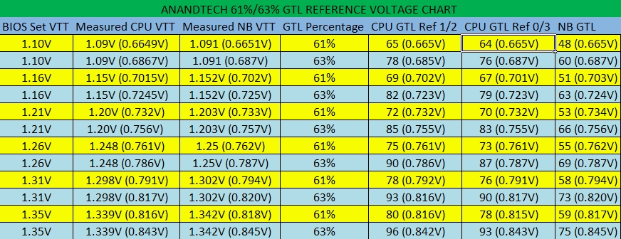
DFI's approach to providing the user with ultra fine control of GTL reference voltages is unsurpassed in the motherboard industry, although working with an ultra fine scale such as this requires a significant dedication of time in order to get things right. In fact, some users enjoy this type of tweaking while others may feel it is akin to pulling teeth. In order to address this situation DFI has gone to the trouble of releasing a scale showing equivalent VTT/GTL percentages and associated BIOS settings.
We have found the scales themselves to be quite broad in range so we are providing a condensed version, taken from measurements using our own board here in the lab. The major issue here is that no two boards/CPUs are likely to behave in the exact same manner. This being the case, the small chart below is only intended to provide a starting point for any adjustments that may need to be made to your particular setup.
 |
Easy
500FSB E8500 Setup guide (easy starting point)
In order to make things as easy and presentable as possible we decided to provide users with a video setup guide showing how to run 500FSB with an Intel E8500 processor. We cannot guarantee the settings shown in the video will work on all systems as component choices will play a huge part in how far the board can clock. Secondly, GTL values vary from board to board and across processors adding further variables in to the mix. We attempted to keep the setup as simple as possible whilst enabling all key chipset registers for performance. If there is enough demand, we may venture into a quad-core overclocking guide too - although 400-420FSB is attainable with a minimum of BIOS level adjustments, so a guide is not really necessary.


24 Comments
View All Comments
Ephebus - Tuesday, April 29, 2008 - link
I remember a time when I was considering the purchase of a midrange ASUS motherboard with a reasonable set of overclocking options in the BIOS but no PCI-E clock setting, and there was no information on the specifications page or the manual as to how that setting would behave when overclocking. I then wrote to ASUS asking if the PCI-E clock was always locked by the board at 100 or if it would vary according to the CPU clock setting, and was actually told by an ASUS support "technician" to "go read a book on overclocking". I managed to get the info later on a forum from a person who owned the board and was kind enough to check it out for me. And that is, when ASUS support doesn't simply delete your support inquiry.With DFI I've managed to actually have short conversations with the technical support staff in the past, was able to report minor BIOS bugs and see them fixed on the next release, etc., so at least for me it's not just a question of whether a DFI motherboard can reach a few MHz more than an ASUS competitor or not on this or that benchmark, it's also all about the feeling of satisfaction from owning a product made by a company that has this kind of attitude towards users, and that always does their best to meet the needs and wishes of enhusiasts. I'll gladly pay more for a DFI product anytime.
Intelman07 - Monday, April 28, 2008 - link
Is there a reason Anandtech reconmends ~400FSB for quad core, does a lower multiplier and a higher FSB increase performance more in a quad core chip?Rajinder Gill - Monday, April 28, 2008 - link
Hi Intelman07,This applies in relation to the FSB limits of the quad cores only ON THIS board; 400 FSB at a trd running near 5-6 will give you a read delay time of around 13ns. Anything over 420 FSB needs a hike in trd while 440+ you need to be looking twoards a trd of 8 which is a delay of 17ns. The drop in write/copy speed bandwidth by reverting to 400FSB is only 500mbs while reads gain 500mbs running the lower tRD (swings and roundabouts). Now factor the VTT and VMCH requiremnts of the higher FSB and it becomes to click.
For more insight into this, 2 of our articles here will explain the fundammnetals and reasoning a little better.
http://www.anandtech.com/mb/showdoc.aspx?i=3208&am...">http://www.anandtech.com/mb/showdoc.aspx?i=3208&am...
and also logical approach to system tuning using Kris' excellent groundwork.
http://www.anandtech.com/cpuchipsets/showdoc.aspx?...">http://www.anandtech.com/cpuchipsets/showdoc.aspx?...
Other boards which vcan hit higher FSB's and low tRDs change these rules a little. But for the most part, the truth is that FSB overcloking on the quads and Joe Public - 400FSB really is realistic and attainable with real stability - and this is important to a majority of our readers. Of course, we still use our cascades from time to time and hammer the boards real hard without any of the logic written here applied.
The interetsing part comes as no surprise - yup - this all favors unlocked multiplier processors aka QX9650 and 9770 class, just up the FSB - keep the tRD low and hey presto!
The beauty of this board is that it gets close to that tRD 12.5ns latency time at 400FSB at 1.25VMCH and 8GB of memory with no need for GTL tuning- easy as pie- with performance that you can't swing anywhere else using a 12mb cache quad on this board.
Hope that clears it up a little..
regards
Raja
Bozo Galora - Monday, April 28, 2008 - link
Another great article by AT's best reviewer.I have read somewhere DFI's top X48 board gonna have ICH10R and cost ~$400??
Slash3 - Monday, April 28, 2008 - link
Page 2 states "The expansion slot layout is comprised of three PCI Express x16 slots (two x16 and one x4 slot), and three PCI slots."The board itself has 3 physical PCI-E 16x slots and 1 PCI-E 4x slot though, so the sentence is kind of ambiguous.
takumsawsherman - Monday, April 28, 2008 - link
It's the wicked fast 400Mbps version, rather than 800Mbps. Wouldn't want to advance the field. Nope, let's use the 10 year old ancient variety, rather than the 5 year old less ancient variety.I've got an even better idea... Why not throw in some USB 1.1 ports.
Rob94hawk - Monday, April 28, 2008 - link
I got all excited and then I saw DDR2....Might as well just replace PCIE with AGP while their at it.
Rajinder Gill - Monday, April 28, 2008 - link
Just contacted DFI, they are aiming at retail launch of the DDR3 version on the 20th May..Review sample boards should ship within the next week..
regards
Raja
Rajinder Gill - Monday, April 28, 2008 - link
EDIT: Make that early June for full retail (allowing for shipping time etc)..regards
Raja
Rob94hawk - Wednesday, April 30, 2008 - link
Will be looking forward to it. Thank you.