DFI X48 LT T2R: Floats like a Butterfly…
by Rajinder Gill on April 28, 2008 4:00 AM EST- Posted in
- Motherboards
Toe to Toe with the BIOS (cont'd)
 |
 |
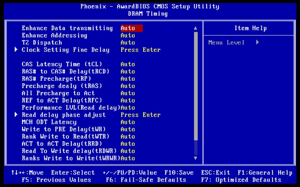
Regardless of individual memory timing preferences, to obtain best RAM/chipset latency performance we recommend that the following BIOS functions be set as follows for Micron D9-based RAM modules.
Enhance Data Transmitting: FAST
FAST MODE: Gives latency and bandwidth improvements over the "Normal" setting without overly affecting memory stability or FSB overclocking potential throughout the frequency ranges of interest for everyday use.
TURBO MODE: More suited to benchmarking runs. This is a very aggressive setting, further improving latencies past "Fast" mode. Using "Turbo" mode may require that the "CH1CH2 Common CLK Crossing Setting" be set to "Nominal" rather than "More Aggressive". VNB requirements are 1.7V and upwards, hence this should be used strictly for short-term benchmarking.
Enhance Addressing: FAST
This brings additional gains of latency and bandwidth used in combination with the above setting for best overall system performance. Again, the stability/voltage requirement hit is only minor for normal PC use. Although the BIOS defaults to Normal mode for both settings, there is no reason to veer away from setting FAST for both functions, provided you're using reasonable memory.
T2 Dispatch: Set this to Disabled, as it gives more overall stability when memory is clocked to high speeds.
 |
Channel 1 CLK Crossing Setting: More Aggressive
Channel 2 CLK Crossing Setting: More Aggressive
CH1CH2 Common CLK Crossing Setting: More Aggressive
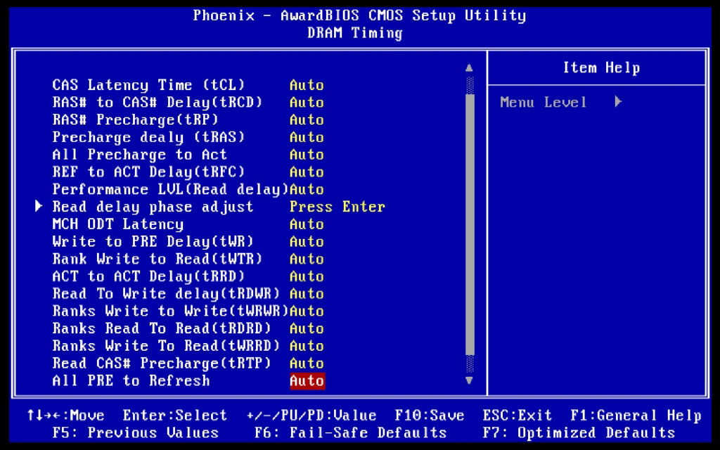
24/7 systems using Micron D9GMH-based modules will certainly want to take advantage of using all three of these settings in unison for a latency and bandwidth boost. We have found these three functions set to "More Aggressive" do not hinder the boards FSB progress excessively. Other RAM modules may not fare as well, unfortunately. Given the choice between a hike in tRD (performance level) or setting the clock crossing settings less aggressively, always strive to maintain the lowest tRD possible. Taking a hit in the clock crossing setting is not as drastic as additional clock delays to the tRD transfer cycle.
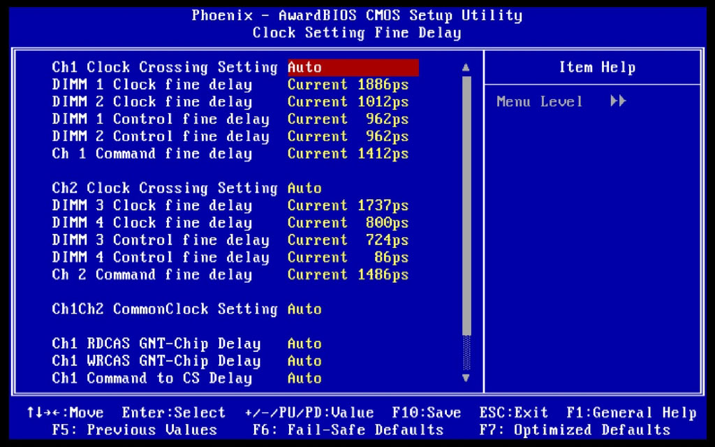
Clock Fine Delays: For both channels, the BIOS adjusts these values automatically when set to CURRENT mode. The scale runs in picoseconds of delay for each setting/channel. Generally, engineers do a very good job of ensuring PCB trace lengths to each DIMM slot on the motherboard are of equal length. Slot 4 is around 3 cm or so from slot 1, so the traces running to DIMM slot 1 will often be "snaked" back across themselves in a U shape to add length to the trace and help eliminate parasitic capacitance issues when running two traces in parallel. The delay functions offer adjustment to help eliminate trace length mismatches ensuring data requests from the MCH are received and dispatched in unison when requested from the appropriate DIMM banks.
Although the BIOS does an admirable job of sensing the delay values required, we found that pushing the board requires some manual tuning of these settings. The Control Fine Delay values for each channel can often be left at Current, while tuning the Clock Fine Delay and Command Fine Delay Settings for both channels is certainly fruitful (depending also on which DIMM slots are occupied by modules). For the most part the delay in picoseconds between each bank should not exceed 70ps or so. Command Fine Delay seems to function best when set to around a 50% value of Clock Fine Delay.
The best way to monitor these settings is to write down the values at default (Current), if the board is stable. As you increase the FSB and hence change the memory frequency, the current values tend to drift away from their ideal or stable settings. To get around this, users can manually apply the settings shown for a stable overclock and tune the board for better stability by making small adjustments to the manually applied values. Do note however, that the values shown by the current settings are not available in the manual adjustment scale, so we must pick the closest value.
At times, the BIOS may select a Command Fine Delay setting that is wholly inadequate for the frequency applied. Often a value under 100ps may be selected, resulting in the board failing to boot into the OS, simply setting this value back to near 50% of the Clock Fine Delay value of Channel 1&3 often results in a "fix".


24 Comments
View All Comments
Ephebus - Tuesday, April 29, 2008 - link
I remember a time when I was considering the purchase of a midrange ASUS motherboard with a reasonable set of overclocking options in the BIOS but no PCI-E clock setting, and there was no information on the specifications page or the manual as to how that setting would behave when overclocking. I then wrote to ASUS asking if the PCI-E clock was always locked by the board at 100 or if it would vary according to the CPU clock setting, and was actually told by an ASUS support "technician" to "go read a book on overclocking". I managed to get the info later on a forum from a person who owned the board and was kind enough to check it out for me. And that is, when ASUS support doesn't simply delete your support inquiry.With DFI I've managed to actually have short conversations with the technical support staff in the past, was able to report minor BIOS bugs and see them fixed on the next release, etc., so at least for me it's not just a question of whether a DFI motherboard can reach a few MHz more than an ASUS competitor or not on this or that benchmark, it's also all about the feeling of satisfaction from owning a product made by a company that has this kind of attitude towards users, and that always does their best to meet the needs and wishes of enhusiasts. I'll gladly pay more for a DFI product anytime.
Intelman07 - Monday, April 28, 2008 - link
Is there a reason Anandtech reconmends ~400FSB for quad core, does a lower multiplier and a higher FSB increase performance more in a quad core chip?Rajinder Gill - Monday, April 28, 2008 - link
Hi Intelman07,This applies in relation to the FSB limits of the quad cores only ON THIS board; 400 FSB at a trd running near 5-6 will give you a read delay time of around 13ns. Anything over 420 FSB needs a hike in trd while 440+ you need to be looking twoards a trd of 8 which is a delay of 17ns. The drop in write/copy speed bandwidth by reverting to 400FSB is only 500mbs while reads gain 500mbs running the lower tRD (swings and roundabouts). Now factor the VTT and VMCH requiremnts of the higher FSB and it becomes to click.
For more insight into this, 2 of our articles here will explain the fundammnetals and reasoning a little better.
http://www.anandtech.com/mb/showdoc.aspx?i=3208&am...">http://www.anandtech.com/mb/showdoc.aspx?i=3208&am...
and also logical approach to system tuning using Kris' excellent groundwork.
http://www.anandtech.com/cpuchipsets/showdoc.aspx?...">http://www.anandtech.com/cpuchipsets/showdoc.aspx?...
Other boards which vcan hit higher FSB's and low tRDs change these rules a little. But for the most part, the truth is that FSB overcloking on the quads and Joe Public - 400FSB really is realistic and attainable with real stability - and this is important to a majority of our readers. Of course, we still use our cascades from time to time and hammer the boards real hard without any of the logic written here applied.
The interetsing part comes as no surprise - yup - this all favors unlocked multiplier processors aka QX9650 and 9770 class, just up the FSB - keep the tRD low and hey presto!
The beauty of this board is that it gets close to that tRD 12.5ns latency time at 400FSB at 1.25VMCH and 8GB of memory with no need for GTL tuning- easy as pie- with performance that you can't swing anywhere else using a 12mb cache quad on this board.
Hope that clears it up a little..
regards
Raja
Bozo Galora - Monday, April 28, 2008 - link
Another great article by AT's best reviewer.I have read somewhere DFI's top X48 board gonna have ICH10R and cost ~$400??
Slash3 - Monday, April 28, 2008 - link
Page 2 states "The expansion slot layout is comprised of three PCI Express x16 slots (two x16 and one x4 slot), and three PCI slots."The board itself has 3 physical PCI-E 16x slots and 1 PCI-E 4x slot though, so the sentence is kind of ambiguous.
takumsawsherman - Monday, April 28, 2008 - link
It's the wicked fast 400Mbps version, rather than 800Mbps. Wouldn't want to advance the field. Nope, let's use the 10 year old ancient variety, rather than the 5 year old less ancient variety.I've got an even better idea... Why not throw in some USB 1.1 ports.
Rob94hawk - Monday, April 28, 2008 - link
I got all excited and then I saw DDR2....Might as well just replace PCIE with AGP while their at it.
Rajinder Gill - Monday, April 28, 2008 - link
Just contacted DFI, they are aiming at retail launch of the DDR3 version on the 20th May..Review sample boards should ship within the next week..
regards
Raja
Rajinder Gill - Monday, April 28, 2008 - link
EDIT: Make that early June for full retail (allowing for shipping time etc)..regards
Raja
Rob94hawk - Wednesday, April 30, 2008 - link
Will be looking forward to it. Thank you.