ASUS ROG Rampage Formula: Why we were wrong about the Intel X48
by Kris Boughton on January 25, 2008 4:30 AM EST- Posted in
- Motherboards
BIOS Screenshots and Interesting Settings
ASUS boards are known for their high level of customization and the Rampage Formula is no exception. The main menu that provides a majority of the options normally associated with overclocking is renamed "Extreme Tweaker", which we feel is entirely appropriate. Users can adjust everything from here, from bus speeds to voltages and memory timings to MCH parameters. Although a few options with indeterminate purposes still exist (for example, "Ai Clock Twister"), for the most part ASUS has done an excellent job in clearly labeling what each setting does.
The ASUS Rampage Formula comes with official FSB1600 support, a feature attached to the use of the upcoming X48 chipset release. Those that want to use the next Intel Core 2 Extreme, the QX9770, will need to buy a board built around X48 if they want a platform validated for 400MHz FSB operation. We found the Rampage required no additional MCH voltage when running at this FSB setting.
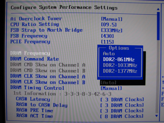
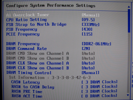
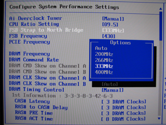
The standard compliment of DDR2 dividers is included in the Rampage Formula's BIOS. We will go into more detail about these later in the review. In any case, even with the fastest DDR2 available, we are not left wanting when it comes to options for pushing our memory.
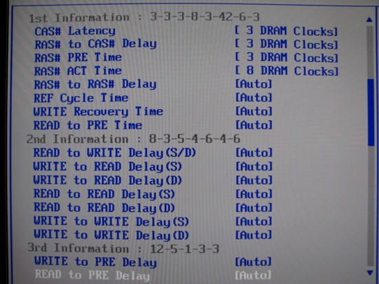
The BIOS includes adjustment options for all primary memory timings - 20 in all. Most of the time a majority of these can be set to "Auto" - ASUS' tuning is already quite good. However, experienced users and memory experts alike will enjoy the expansive level of control allowed.
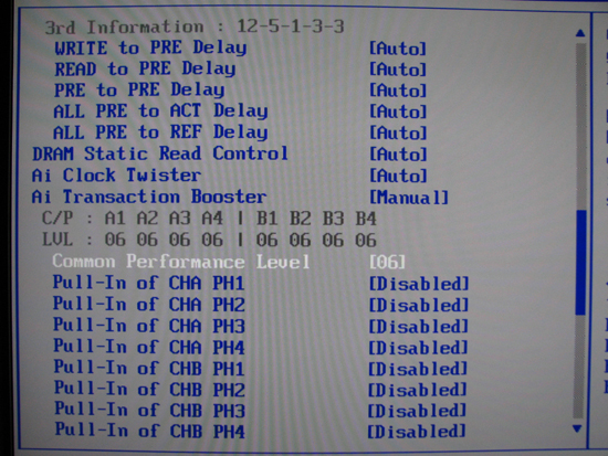
Here we can get a good look at what we consider the most significant change to the standard ASUS BIOS offering in years. "Common Performance Level", more correctly known as MCH Read Delay (tRD), allows the user to specifically establish a desired value, something that was not entirely possible in the past. Earlier versions of "Ai Transaction Booster" only allowed the user to apply an offset, which made controlling tRD difficult when the base value was unknown.
Additionally, each FSB bus cycle "phase" for each channel can be further manipulated. "CHA" and "CHB" refer to the two independent memory channels in a dual-channel memory configuration. Installing only one memory DIMM, or certain combinations of mismatched memory module pairings across all four expansion slots, results in the motherboard defaulting to single-channel operation; otherwise there are two memory channels in operation, which enhances overall system performance. The number of phases per channel depends on the memory divider in use (each channel will always have the same number of channels though) - a 3:2 memory divider has two phases, 4:3 has three, and 8:5 has five, for example. We will explore the theory behind this truth shortly.
Setting a single channel/phase "Pull-In" to enabled has the effect of lowering that particular phase's associated tRD value to one below the Common Performance Level (the "base" tRD). Leaving the setting disabled leaves the phase unadjusted, in which case it is the same as the base tRD. Much like memory timings, lower tRD values bring greater performance. As we will see, these settings primarily allow users to squeeze out any unclaimed performance benefit possible with the current tRD when the next "lower" Common Performance Level is unachievable. Do not feel as though you need to understand what all of this means right now, as we will cover all of this and much more in excruciating detail soon enough.
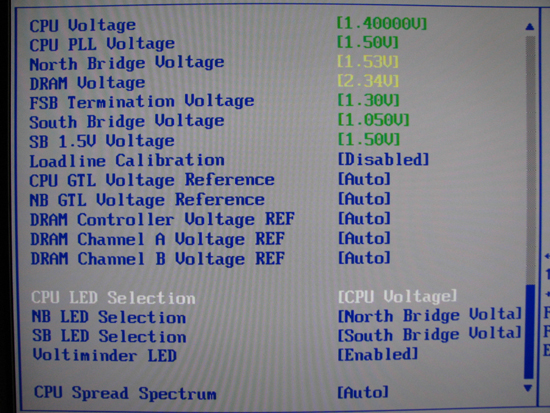
With no less than seven onboard voltage adjustments, the Rampage Formula is a tweaker's dream come true. Because ASUS motherboards do make a habit of "adjusting" some of these values automatically at times, we recommend you manually set all voltages to the bottom of their ranges unless otherwise required. This best practice just makes good sense and ensures nothing receives more voltage than intended by the user. Again, we must also strongly caution against the use of "Loadline Calibration." We recommend you leave this option disabled, especially when installing a 45nm CPU.
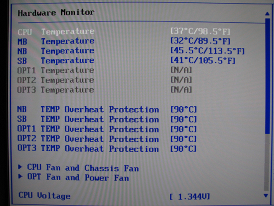
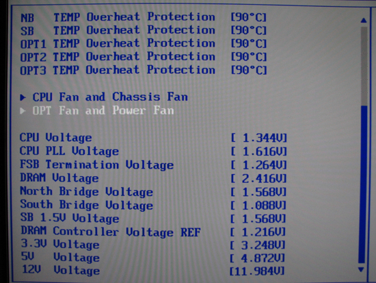
ASUS' implementation of their in-BIOS hardware monitor is extremely informative. You can simultaneously check temperatures for the CPU, motherboard (PWM), Northbridge (NB), and Southbridge (SB) as well as quickly review the effect that prior voltage adjustments had on actual voltage levels. Although we found most reported voltages were fairly accurate, obtaining the most precise readings possible still requires the use of a digital multimeter (DMM).
Regarding voltages, we found two concerns worth mentioning. Firstly, the reported CPU PLL voltage appears to be non-functional as it always reads the same, regardless of setting. Second, like many other ASUS offerings the motherboard consistently overvolts the memory by 0.08 ~ 0.10V. We do not see any real problem with this, as long as the user is aware it's happening.


73 Comments
View All Comments
xieper - Saturday, August 22, 2009 - link
Did that article ever materialise? I have not been able to find it anywhere on this site....papatsonis - Sunday, May 16, 2010 - link
way too late for this.. (cause i actually calculate the allowable tRDs "on the fly") but may be useful for some, this little excel which calculates the minimum allowable tRDhttp://rapidshare.com/files/388032472/DDR2_tRD_Cal...
papatsonis - Sunday, May 16, 2010 - link
some small changes/additionshttp://rapidshare.com/files/388191811/DDR2_tRD_Cal...