Overclocking Intel's New 45nm QX9650: The Rules Have Changed
by Kris Boughton on December 19, 2007 2:00 AM EST- Posted in
- CPUs
The Origins of Static Read Control Delay (tRD)
With over a year of experience overclocking the Core 2 family of processors, we have learned a thing or two. One of the most important items we've learned is that higher FSB settings do not necessarily mean better performance. Understandably, this may come as a shock to some. For whatever reason, even a lot of well-regarded, seasoned overclockers seem to place great value in achieving the highest possible FSB. Based on what we know, we always establish our base target MCH overclock at the same spot - 400MHz FSB with a tRD of 6. The only other potential base MCH target value even worth considering is 450MHz with a tRD of 7, which should only be used when extra memory speed is needed or when a low maximum CPU multiplier becomes a limiting factor. Without getting into too much detail, let's examine what we mean by this.
When it comes to overclocking, the MCH functions as a hybrid of sorts. Like a CPU, it has an upper frequency limit and more voltage can often raise this limit. On the other hand, since it interfaces with memory it also behaves somewhat like memory with internal "timings" whose absolute values derive from the established FSB.
Consider the case of memory rated to run DDR-800 at CAS 3. We can calculate the absolute CAS (Column Address Strobe) delay in a few quick steps. DDR-800, which is in fact double date rate as the name suggests, runs at a base frequency of 400MHz or 400 million cycles per second. Inverting this value tells us the number of seconds per cycle (2.50ns). Finally, multiplying this by the CAS rating tells us the total delay time of 7.5ns (3 x 2.5ns). Likewise, setting a CAS value of 4 results in an absolute CAS delay of 10ns. We can see now why higher CAS values give way to lower memory bandwidths - in the case described above the MCH spends more time "waiting" for data to become available when the memory is set to CAS 4.
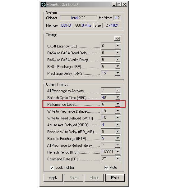
tRD in hiding…we promise we didn't make up the horrible "Performance Level" moniker
Arguably, the most important MCH setting when it comes to performance tweaking is the Static Read Control Delay (tRD) value. Like the memory CAS (CL), setting this value is relative to FSB. Case in point, a tRD value of 6, calculated in the same manner as used before, tells us that MCH sets a read delay of 15ns at an FSB of 400MHz. This means that in addition to the time required for the CPU to issue a request for data in memory to the MCH, the time the MCH spends translating and issuing the command to the memory, and the time the memory requires in retrieving the requested data, the MCH will spend an additional 15ns simply waiting for valid data to become available before fulfilling the CPU's original read request. Obviously, anything that can minimize this wait will be beneficial in improving memory read bandwidth and quite possibly overall system performance.
Until recently, direct tRD manipulation by the user was not even possible. In fact, for the longest time BIOS engineers had no choice but to accept this setting as essentially "hard-coded", making MCH performance rather lackluster. The only way to increase memory subsystem performance was to run at higher FSB settings or tighten primary memory timings. At some point, the MCH design teams got tired of the CPU people hogging all the glory and in a well-calculated effort to boost MCH performance exposed this setting for external programming.
The outside world's first introduction to variable tRD settings came when a few overclockers noticed that setting lower MCH "straps" allowed for higher memory bandwidths. What they didn't know at the time was that they had unintentionally stumbled upon tRD. Tricking the motherboard into detecting an installed CPU as an 800 FSB (200MHz) part forced the MCH into setting a lower tRD value than if the FSB were 1066 (266MHz). Consequently, overclocking the system to the same higher FSB value with the lower strap setting yielded higher memory performance. Often times the effect was significant enough that real-world performance was higher even with a lower final FSB. The tradeoff was apparent however: a lower strap meant a lower maximum FSB. The MCH tRD value, just like a memory timing, must eventually be loosened in order to scale higher. What's more, as is the case with memory, additional voltage can sometimes allow the MCH to run with tighter "timings" at higher speeds.
Eventually the inevitable next step in memory performance tuning became a reality. The option to adjust tRD independent of MCH strap selection became part of every overclocker's arsenal. Nowadays the MCH strap setting does little more than determine which memory multiplier ratios are available for use. Although tRD adjustments are now possible in many BIOS implementations, some motherboard manufactures choose to obfuscate their true nature by giving the setting confusing, proprietary names like "Transaction Booster" and the like. Don't let these names fool you; in the end they all do the same thing: manipulate tRD.


56 Comments
View All Comments
Lifted - Wednesday, December 19, 2007 - link
Very impressive. Seems more like a thesis paper than a typical tech site article. While the content on AT is of a higher quality than the rest of the sites out there, I think the other authors, founder included, could learn a thing or two from an article like this. Less commentary/controversy and more quality is the way to go.AssBall - Wednesday, December 19, 2007 - link
Shouldn't page 3's title be "Exlporing the limits of 45nm Halfnium"? :Dhttp://www.webelements.com/webelements/elements/te...">http://www.webelements.com/webelements/elements/te...
lifeguard1999 - Wednesday, December 19, 2007 - link
"Do they worry more about the $5000-$10000 per month (or more) spent on the employee using a workstation, or the $10-$30 spent on the power for the workstation? The greater concern is often whether or not a given location has the capacity to power the workstations, not how much the power will cost."For High Performance Computers (HPC a.k.a. supercomputers) every little bit helps. We are not only concerned about the power from the CPU, but also the power from the little 5 Watt Ethernet port that goes unused, but consumes power. When you are talking about HPC systems, they now scale into the tens-of-thousands of CPUs. That 5 Watt Ethernet port is now a 50 KWatt problem just from the additional power required. That Problem now has to be cooled as well. More cooling requires more power. Now can your infrastructure handle the power and cooling load, or does it need to be upgraded?
This is somewhat of a straw-man argument since most (but not all) HPC vendors know about the problem. Most HPC vendors do not include items on their systems that are not used. They know that if they want to stay in the race with their competitors that they have to meet or exceed performance benchmarks. Those performance benchmarks not only include how fast it can execute software, but also how much power and cooling and (can you guess it?) noise.
In 2005, we started looking at what it would take to house our 2009 HPC system. In 2007, we started upgrades to be able to handle the power and cooling needed. The local power company loves us, even though they have to increase their power substation.
Thought for the day:
How many car batteries does it take to make a UPS for a HPC system with tens-of-thousands of CPUs?
CobraT1 - Wednesday, December 19, 2007 - link
"Thought for the day:How many car batteries does it take to make a UPS for a HPC system with tens-of-thousands of CPUs?"
0.
Car batteries are not used in neither static nor rotary UPS's.
tronicson - Wednesday, December 19, 2007 - link
this is a great article - very technical, will have to read it step by step to get it all ;-)but i have one question that remains for me.. how is it about electromigration with the very filigran 45nm structures? we have here new materials like the hafnium based high-k dielectricum, guess this may improove the resistance agains em... but how far may we really push this cpu until we risk very short life and destruction? intel gives a headroom until max 1.3625V .. well what can i risk to give with a good waterchill? how far can i go?
i mean feeding a 45nm core p.ex. 1,5V is the same as giving a 65nm 1,6375! would you do that to your Q6600?
eilersr - Wednesday, December 19, 2007 - link
Electromigration is an effect usually seen in the interconnect, not in the gate stack. It occurs when a wire (or material) has a high enough current density that the atoms actually move, leading to an open circuit, or in some cases, a short.To address your questions:
1. The high-k dielectric in the gate stack has no effect on the resistance of the interconnect
2. The finer features of wires on a 45nm process do have a lower threshold to electromigration effects, ie smaller wires have a lower current density they can tolerate before breaking.
3. The effects of electromigration are fairly well understood at this point, there are all kinds of automated checks built in to the design tools before tapeout as well as very robust reliability tests performed on the chips prior to volume production to catch these types of reliability issues.
4. The voltage a chip can tolerate is limited by a number of factors. Ignoring breakdown voltages and other effects limited by the physics of transistor operation, heat is where most OC'ers are concerned. As power dissipation is most crudely though of in terms of CVf^2 (capacitance times voltage times frequency-squared), the reduced capacitance in the gate due to the high-k dielectric does dramatically lower power power dissipation, and is well cited. The other main component in modern CPU's is the leakage, which again is helped by the high-k dielectric. So you should expect to be able to hit a bit higher voltage before hitting a thermal envelope limitation. However, the actual voltage it can tolerate is going to depend on the CPU and what corner of the process it came from. In all, there's no general guideline for what is "safe". Of course, anything over the recommended isn't "safe", but the only way you'll find out, unfortunately, is trial and error.
eilersr - Wednesday, December 19, 2007 - link
Doh! Just noticed my own mistake:high-k dielectric does not reduce capacitance! Quite the contrary, a high-k dielectric will have higher capacitance if the thickness is kept constant. Don't know what I was thinking.
Regardless, the capacitance of the gate stack is a factor, as the article mentioned. I don't know how the cap of Intel's 45nm gate compares with that of their 65nm gate, but I would venture it is lower:
1. The area of the FET's is smaller, so less W*L parallel plate cap.
2. The thickness of the dielectric was increased. Usually this decreases cap, but the addition of high-k counter acts that. Hard to say what balance was actually achieved.
This is just a guess, only the process engineers no for sure :)
kjboughton - Wednesday, December 19, 2007 - link
Asking how much voltage can be safetly applied to a (45nm) CPU is a lot like asking which story of a building can you jump from without the risk of breaking both legs on the landing. There's inherent risk in exceeding the manufacturer's specification at all and if you asked Intel what they thought I know exactly what they would say -- 1.3625V (or whatever the maximum rated VID value is). The fact of the matter is that choices like these can only be made by you. Personally, I feel exceeding about 1.4V with a quad 45nm CPU is a lot like beating your head against a wall, especially if your main concern is stability. My recommendation is that you stay below this value, assuming you have adequate cooling and can keep your core temperatures in check.renard01 - Wednesday, December 19, 2007 - link
I just wanted to tell you that I am impressed by your article! Deep and practical at the same time.Go on like this.
This is an impressive CPU!!
regards,
Alexander
defter - Wednesday, December 19, 2007 - link
People stop posting silly comments like: "Intel's TDP is below real power consumption, it isn't comparable to AMD's TDP".Here we have a 130W TDP CPU consuming 54W under load.