ASUS Maximus Extreme - the Extreme Benchmarker's Choice?
by Rajinder Gill on December 10, 2007 8:00 AM EST- Posted in
- Motherboards
Important BIOS Functions
We have picked out a few of the more important BIOS functions for a breakdown of their use and application. The "Advanced Tweaker" BIOS screen has quite a few secondary memory timing options; for the most part these can be left to board/SPD default values. We are providing the best "bang for the buck" manual settings below.
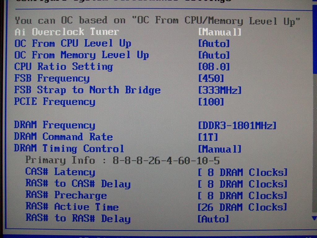 |
AI Overclock Tuner: Set this function to manual for overclocking; the Auto function enables preset overclocks automatically when the system is under load.
OC from CPU Level Up: ASUS enabled overclock profiles based upon the processor type in use; for manual overclocking, leave this function at Auto. If low level automatic preset overclocking is preferred, select either the CPU type or "Crazy" mode. Setting either of the latter two options adjusts all board voltages to preset values. The preset values themselves can be higher than is absolutely necessary for the applied overclock. The Auto overclock functions can be useful for beginners who are getting to grips with overclocking, with the option to move to manual overclocking later. We suppose this guarantees stability via a somewhat brute force approach. For long-term use, we recommend using a manually set overclock.
FSB Strap to Northbridge: Unlike older chipsets, performance hits of using the higher MHz Northbridge straps are virtually non-existent. Synthetic latency and read figures across any of the 266/333 or 400 straps are almost identical. There are small variances in overall stability, for quad processors running over 400FSB - the 333 and 400 straps worked better for us. For benching with dual-core CPUs, we found the 266 strap allowed us sufficient overhead to run the board up to 550 FSB. Between 550-575 FSB, we were limited to the 333 and 400 NB straps depending on memory timings. The 200 NB setting offers inadequate FSB potential to consider it worthy of use with Intel's latest processors.
PCI-E Frequency: If the ICH9R SATA ports are used then a setting around 115 MHz is safe, though scores do not seem affected by the minimal 15MHz overclock. We noticed anything over 118MHz would cause problems with the drives or even the POST routines. Benchmarkers as usual are best off using an IDE drive, turning off all the peripherals, and then trying to maximize the bus speed.
DRAM Frequency: The available dividers for the 266/333/400 NB straps are:
| NB Staps and Dividers | |
| 266 | 4:5/2:3/1:2 |
| 333 | 1:1/5:6/5:8/1:2 |
| 400 | 1:1/3:4/1:2 |
DRAM Command Rate: Sets either 1N or 2N memory timing. Our test sample is perfectly capable of holding 1N command rate at up to DDR3-1840Mhz. The synthetic performance advantage of 1N over 2N is around ~1.8ns (1-3%). As the board has no issue using 1N at high speeds, it becomes almost mandatory to set 1N for all overclocking.
DRAM Timing Control: Set this to Manual to obtain control of all primary and secondary memory timing ranges. The BIOS shows primary and secondary timings above both respective timing sections. Users may wish to enter the shown timings manually for each setting and then experiment with tighter timings where possible. The board defaults are generally tight enough for 24/7 use. For benchmarking, Memset allows access to setting ranges that are not accessible in BIOS. We look at a few timing ranges below.
RAS To RAS Delay: The BIOS generally defaults to 4 for this setting; for benchmarking, we have used 3. At high FSB speeds, a setting of 5 may provide more stability with the counter effect of a small loss in performance.
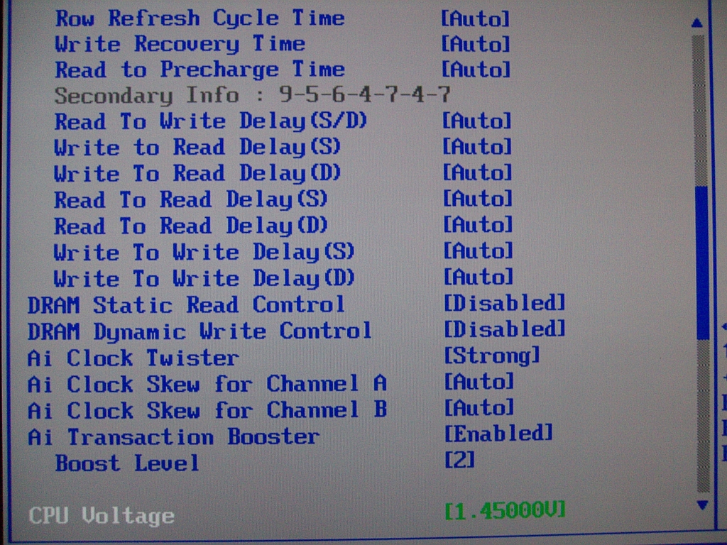 |
Row Refresh Cycle Time - aka TRFC: For benchmarking TRFC can be set as low as 45-50; if shooting for stability values of 60 and above are fine. A lower setting gives big gains in bandwidth and can affect benchmarking scores quite drastically.
Write Recovery Time: Default value here is 8. This setting works fine over a broad range of FSB and memory speeds. If stability issues are experienced, it may be worth experimenting with a setting of 9. Lower is tighter and gives small gains in memory write performance.
Read to Precharge Time: A range of 3-6 is usable. For stability testing with high RAM speeds in excess of DDR3-1700, 1N command rate may require a setting of 6. For benchmarking, values as low as 3 are possible, though stability will be dependent on the benchmark in question. A setting of 3 applied via Memset is best.
DRAM Static Read Control and DRAM Dynamic Write Control: Both these functions are best set to 'Disabled' for overclocking. We could not substantiate any significant memory bandwidth or latency gains using the 'Enabled' setting. Further, setting 'Enabled' may actually hinder overclock success.
AI Clock Twister: We recommend use of the "Strong" setting wherever possible. Setting "Weak" reduces overall bandwidth and access latency.
Transaction Booster: Ranges here are from 1-8 (1-3 are usable changes in BIOS), with either the "Enabled" or "Disabled" setting. A setting of 1 with "Enabled" selects the default tRD level for the NB strap and memory divider combination. Each digit increase to the Transaction Booster with the "Enabled" setting will subtract 1 from Performance Level, providing us with higher memory bandwidth and lower access latency. The "Disabled" function inreases tRD (tRD +1) and/or tRD phases with each additional digit over 1, meaning an upward scale increase or boost is less aggressive with Transaction Booster set to "Disabled".
AI Clock Skew Channel A and Channel B: Timing unison between both channels of memory is essential for stability. PCB trace length variance between Channel A and Channel B can lead to an offset of signaling between both Channels. Delaying Channel A or advancing Channel B may be required to realign clock timing at high memory speeds - thus improving stability. Generally, we used either a delay of 50-100ps on Channel A with Channel B set to "Normal". Alternately, we can advance Channel B by 50-100ps with Channel A set to "Normal". Users may need to experiment between various levels of "Skew" to find optimal settings.


27 Comments
View All Comments
retrospooty - Monday, December 10, 2007 - link
Wireless works yes. They are linked up through the base and work in dos mode. Both RF, and bluetooth meese work.kilkennycat - Monday, December 10, 2007 - link
I notice from the board picture that the rear mounting holes are still in the corners of the board, so if the WIDTH is 4cm more than the standard ATX, does the board need special mounting ? I assume that WIDTH means the distance across the edge of the board in contact with the rear of the case. Please correct if my assumption is wrong.Rajinder Gill - Monday, December 10, 2007 - link
THe width is the length across the top edge of the board. Screw hole spacing is still standard ATX, just that this board over-hangs by a few cm (the Sata port end will protrude further into your case) ...regards
Raja
kilkennycat - Monday, December 10, 2007 - link
As yes, you actually mean DEPTH of course, if referencing tower case dimensions (Height x Width x Depth). So any case wishing to accommodate this board needs to have at least 4cm DEEPER front to rear clearance for the motherboard, nothing to do with it being a mid-tower or full-tower. Am I right?Might also preclude using this MB in those cases having the motherboard mounted on a slide-in ATX tray ( a great feature, btw ), as they may have a lip or other registration hardware on the leading-edge of the tray.
retrospooty - Monday, December 10, 2007 - link
What size are they? I cant find it here, or on Asus's site. They look like 1/4 inch - which kind of sucks.Rajinder Gill - Monday, December 10, 2007 - link
The fittings are 1/4", but ASUS does provide adapetrs to use 1/2 tubing..Raja..
retrospooty - Monday, December 10, 2007 - link
thanks... bummer. 1/4 restricts my flow.