NVIDIA nForce4 Ultra: Biostar's Performance Surprise
by Gary Key on February 16, 2006 12:05 AM EST- Posted in
- Motherboards
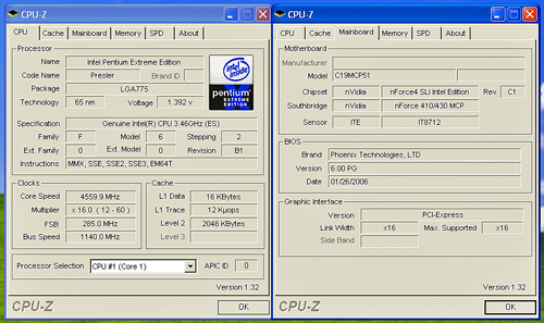
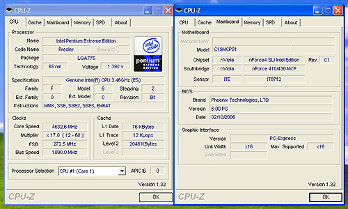
FSB Overclocking Results
Updated 955EE Testing
Memory Stress Testing
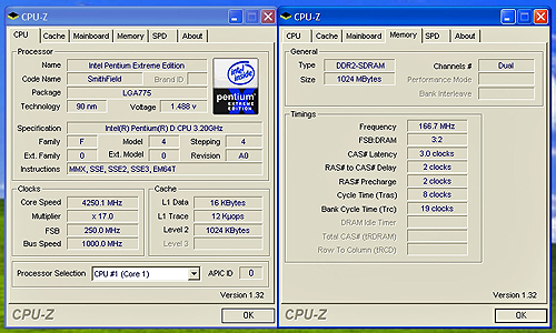
Memory stress tests look at the ability of the Biostar TForce4 U 775to operate at the officially supported memory frequencies of 667MHz DDR2, at the best performing memory timings that the Corsair CM2X512A-5400UL revision 1.3 will support.
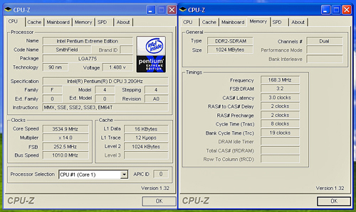
The Biostar TForce4 was very stable with 2 DDR2 modules in Dual-Channel at the settings of 3-2-2-8 at 2.1V. We will now install all four available memory slots that result in more strenuous requirements on the memory subsystem than testing 2 DDR2 modules on a motherboard.
The Biostar TForce4 was completely stable with 4 DDR2 modules in Dual-Channel operation at the settings of 3-3-3-8, but required the command rate to be increased to 2T. We tried several combinations of memory settings at the 3-2-2-8 settings, but the board was not stable enough to complete our test suite.
| Front Side Bus Overclocking Testbed | |
| Processor: | Pentium 4 Smithfield LGA 775 840EE Dual Core 3.2GHz |
| CPU Voltage: | 1.4825V (1.4000V default) |
| Memory Settings: | 3-2-2-8 at 667MHz |
| Memory Voltage: | 2.1V |
| SPP Voltage: | 1.58V |
| FSB Voltage: | 1.40V |
| Cooling: | Thermaltake Big Typhoon |
| Power Supply: | OCZ Power Stream 520 |
| Maximum CPU OverClock: | 250fsb x 17 (4250MHz) +33% |
| Maximum FSB OverClock: | 255fsb x 16 (4092MHz) +27% |

Updated 955EE Testing
Memory Stress Testing
Memory stress tests look at the ability of the Biostar TForce4 U 775to operate at the officially supported memory frequencies of 667MHz DDR2, at the best performing memory timings that the Corsair CM2X512A-5400UL revision 1.3 will support.
| Biostar TForce4 U 775 Stable DDR667 Timings - 2 DIMMs (2/4 slots populated - 1 Dual-Channel Bank) |
|
| Clock Speed: | 200MHz (800FSB) |
| Timing Mode: | 667MHz - Default |
| CAS Latency: | 3 |
| RAS to CAS Delay: | 2 |
| RAS Precharge: | 2 |
| RAS Cycle Time: | 8 |
| Command Rate: | 1T |
| Voltage: | 2.1V |
The Biostar TForce4 was very stable with 2 DDR2 modules in Dual-Channel at the settings of 3-2-2-8 at 2.1V. We will now install all four available memory slots that result in more strenuous requirements on the memory subsystem than testing 2 DDR2 modules on a motherboard.
| Biostar TForce4 U 775 Stable DDR667 Timings - 4 DIMMs (4/4 slots populated - 2 Dual-Channel Banks) |
|
| Clock Speed: | 200MHz (800FSB) |
| Timing Mode: | 667MHz - Default |
| CAS Latency: | 3 |
| RAS to CAS Delay: | 3 |
| RAS Precharge: | 3 |
| RAS Cycle Time: | 8 |
| Command Rate: | 2T |
| Voltage: | 2.10V |
The Biostar TForce4 was completely stable with 4 DDR2 modules in Dual-Channel operation at the settings of 3-3-3-8, but required the command rate to be increased to 2T. We tried several combinations of memory settings at the 3-2-2-8 settings, but the board was not stable enough to complete our test suite.


31 Comments
View All Comments
jamesbond007 - Thursday, February 16, 2006 - link
Haha! Way to go, Gary. You have a fan base! =PGary Key - Thursday, February 16, 2006 - link
Thanks for kind words everyone. I will post a short update to this article in a couple of days as the new bios results are looking promising in resolving some overclock and bios lockup issues.drewintheav - Thursday, February 16, 2006 - link
Gary is awesome! :)Zebo - Thursday, February 16, 2006 - link
I love Gary can't we get him writing articles people will read? Intel/biostar - common.. you'll get 1000 page hits max and 3/4 of them are because Gary wrote it!:PGooger - Thursday, February 16, 2006 - link
Not too bad if you want a P4, but for me I am avoiding nVIDIA Chipsets except when it comes to AMD products. Go Go ULi!DigitalFreak - Thursday, February 16, 2006 - link
Uh, you mean Go Go Nvidia, since they own ULi now...Googer - Thursday, February 16, 2006 - link
Finaly Intel Gets Hypertransport on their chips, like it or not HTT probably is becoming a standard that Intel might have to adopt sooner or later.DigitalFreak - Thursday, February 16, 2006 - link
This has nothing to do with Intel. Nvidia uses HT to communicate between their north and south bridges. They've done it with all their Intel chipsets so far.Googer - Thursday, February 16, 2006 - link
Since the noth bridge has HTT, in theory you could connect an nVIDIA based nFORCE north bridge to a ULi or nVIDIA AMD north bridge and have one of several things:1) A dual CPU system- One Intel Pentium M/4 and One AMD 64 CPU running on the same motherboard simultaniously. The OS might need to be re-written so that multi-threaded applications only use one processor. Linux prehaps?
2) AMD 64 Could get Quad Channel RAM higher.
3) You could ADD a ULi M1567 Southbridge to get True AGP with that PCI-express SLI.
4) You could possibly mix and match chipsets. VIA K8T8xx with one of AMD's north/south bridges and an nFORCE Intel Editon.
You could possibly Connect the AMD 64 Directly (using it's own HTT link) in to the the P4 north bridge with no need to use the chipset designed for the A64.
HTT on Intel means a whole new world of possibilites!
Furen - Thursday, February 16, 2006 - link
Huh? How is Intel getting hypertransport on its chips? HT is a standard but I dont think Intel will ever adopt it because of its pride, more than anything else. It truly doesn't matter though, since HT is just a data transport and using any other data transport gives you the same results as long as it is used in a similar configuration.