SUN’s UltraSparc T1 - the Next Generation Server CPUs
by Johan De Gelas on December 29, 2005 10:03 AM EST- Posted in
- CPUs
The 8 little cores that could
Each core is pretty small, as it has only one pipeline, no Branch Prediction Unit, no OOO buffers, and no OOO pipeline stages, which search for independent instructions. Only the large register file and thread select logic make the very simple core a bit fatter and more complex.
An 8 KB data cache and 16 KB instruction cache give an L1-hitrate of 90% or less, but it also helps to keep each core small. To keep 8 cores with such tiny L1-caches running at 70% efficiency with so many threads, a big L2-cache and massive memory bandwidth is needed.
We have quantified this effect of faster cache coherency in our Linux database server article. A dual core Opteron was about 13% faster than two single core CPUs at the same clock speed. With 8 cores that might share data, cache coherency has an even bigger impact on performance. Sharing the L2-cache also ensures that no coherency traffic is necessary on the level 2 cache.
There is more. Each core has a modular arithmetic unit (MAU) that supports modular multiplication and exponentiation to speed up Secure Sockets Layer (SSL) processing. This compensates for the lack of the FPU and the low clock speed. A single 1.2 GHz MAU seems to "sign" as fast as a 1.8 GHz Opteron, but quite a bit slower at verifying authenticity.
Each core is pretty small, as it has only one pipeline, no Branch Prediction Unit, no OOO buffers, and no OOO pipeline stages, which search for independent instructions. Only the large register file and thread select logic make the very simple core a bit fatter and more complex.
An 8 KB data cache and 16 KB instruction cache give an L1-hitrate of 90% or less, but it also helps to keep each core small. To keep 8 cores with such tiny L1-caches running at 70% efficiency with so many threads, a big L2-cache and massive memory bandwidth is needed.
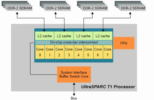
Fig 5: 8 cores fed by a 3 MB L2-cache and 4 integrated memory controllers. Source:SUN.
We have quantified this effect of faster cache coherency in our Linux database server article. A dual core Opteron was about 13% faster than two single core CPUs at the same clock speed. With 8 cores that might share data, cache coherency has an even bigger impact on performance. Sharing the L2-cache also ensures that no coherency traffic is necessary on the level 2 cache.
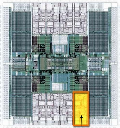
Fig 6: One (yellow) of the 8 cores (gray) of the T1. Source:SUN.
As a rough guideline, performance degrades if the number of floating-point instructions exceeds 1 percent of total instructions.Some instructions like division have long latencies, causing the thread to be skipped. The situation is then similar to a thread with a long latency load. To keep power consumption and die size per core low, each core has a very shallow six-stage pipeline: fetch, thread select, decode, execute, memory, and write back. The result is an architecture that does not need branch prediction, thanks to a shallow pipeline and FMT. However, this limits clock speed to 1.2 GHz in 90 nm, while competing chips are clocking between 2 and 4 GHz.
There is more. Each core has a modular arithmetic unit (MAU) that supports modular multiplication and exponentiation to speed up Secure Sockets Layer (SSL) processing. This compensates for the lack of the FPU and the low clock speed. A single 1.2 GHz MAU seems to "sign" as fast as a 1.8 GHz Opteron, but quite a bit slower at verifying authenticity.


49 Comments
View All Comments
thesix - Friday, December 30, 2005 - link
If you're talking about POWER5's SMT, currently it provides two HW threads per core:http://publib.boulder.ibm.com/infocenter/pseries/i...">http://publib.boulder.ibm.com/infocente...x.doc/ai...
If you look closer at T1, the best one has 8 cores, each core supports four HW threads.
http://www.sun.com/processors/UltraSPARC-T1/">http://www.sun.com/processors/UltraSPARC-T1/
SMT and CMT appear to be the same type of technology (at least conceptual wise) with different names from two vendors.
> The very very poor FP performance of T1 is the truth.
> We have to remind ourselves that it is only a integer CPU. It's FP performance is too terrible.
OK. Since you have repeated so many times, I am sure everyone who's reading this will remember, and I do not disagree :-).
Thanks.
Betwon - Friday, December 30, 2005 - link
We think that it is diffirent between CMT and SMT.For exapmle:
P4 630 is a kind of SMT CPU, but not a CMT CPU.
AthlonX2 is a kind of CMT CPU, but not a SMT CPU.
From anandtech:
T1 has no branch prediction,and it has only one-instruction-issue/core, 8KB L1D/core(too few for 4 threads to use).
POWER5 has 32KB L1D/core, which is used by two threads.
We think that the SMT of T1 may be OK, unless 4 threads only use very few L1D cache(It is impossible for most cases)
Betwon - Friday, December 30, 2005 - link
edit:The only explain about how to improve the efficiency(very poor) is to use SMT to hide the stall's latency(by branch miss/cache miss ect.)
But a core has only 8KB L1(which will be used by 4 threads), the cache miss will increase. It is possible to become worst.
Betwon - Friday, December 30, 2005 - link
edit: T1 have no branch prediction and it has only one_inst_issue/core.Brian23 - Friday, December 30, 2005 - link
Obviously the apps that they used to benchmark in this article like running on the chip. Also, this chip doesn't run windows. It runs Sun's proprietary operating system. (I forgot what it's called.) Sun will give this new chip software support because they want it to do well.I think I read in the article that the chip is backwards compatable with the previous design Sun chips, meaning a lot of software is already available that will run on the chip.
Betwon - Friday, December 30, 2005 - link
NO!It is too narrow for the areas of 32-thread-parallel-well apps.
'have many threads' is not equal to '32-thread-parallel-well'!
Even there are 32 threads, but without parallel-well , This new CPU will waste more than 90% of it's potential.
The efficiency of Itanium( Itanium is capable of a 1.3-1.5 IPC) is much better than x86-CPU(0.7-0.9 IPC). Itanium never used OOO logic and long pipelines.
Betwon - Friday, December 30, 2005 - link
The efficiency of Itanium2 is still better than IBM's POWER5, and a Itanium2 core may retire 6 instrutions/cycle,and POWER5's can retire 5-instrutions/cycle.But a core of this new CPU is only one instrutions/cycle.
Brian23 - Friday, December 30, 2005 - link
I think you missed the part where x86 chips spend 400 cycles waiting on memory accesses when the Sun chip just keeps chugging with another thread while the load is happening.Calin - Tuesday, January 3, 2006 - link
Those 400 cycles are related to the higher clock speed (if your processor would be twice as slow, it would wait only 200 cycles). I assume the 400 cycles are based on the Xeon processor (that has high clock speed and slower FSB).Betwon - Friday, December 30, 2005 - link
NO!It is not true for all the x86 CPU.When Athlon64 spend many cycles waiting on memory accesses,
For P4 with HT,P4 just keeps chugging with another thread while the load is happening.
Do you understand what I want to say?