Intel Core Duo (Yonah) Performance Preview - Part II
by Anand Lal Shimpi on December 19, 2005 12:55 PM EST- Posted in
- CPUs
It's called the Core Duo
When Yonah first started appearing on roadmaps, we knew it as Jonah, which then starting being written as Yonah. Eventually, Intel confirmed its existence and we had always assumed that it would continue to use the name Pentium M. However, given the great importance of the launch of Intel's first dual-core, low power, notebook processor, it shouldn't be much of a surprise that Intel has a new name in store for it. As you've probably already heard, Yonah will receive the marketing name "Core" with the words "Duo" or "Solo" following it depending on whether it is the dual or single core version. The name Centrino will still be there, but instead of referring to the processor as a Pentium M, it'll be called a Core Duo or a Core Solo. The Centrino platform itself will be referred to as Centrino Duo when paired with a Core Duo processor. We have to admit, we kind of like the new name.
Not so pleasant, however, are the new processor numbers that go along with the new processor names. Gone are Intel's simple three-digit numbers and they have since been replaced with a four-digit number preceded by a letter. The letter indicates the thermal envelope of the processor, while the following four digits denote the performance level of the CPU. If you think that this sounds oddly similar to AMD's Turion processor nomenclature, don't worry; you'd be completely right (of course, the Turion only uses two numbers, while Core Duo uses four). Maybe, one of these days, Intel will get around to copying some more important elements of AMD's history, such as an on-die memory controller or at least a serial bus interface.
As an example of the numbers in use, the 2.0GHz processor that we previewed in the first article will be sold under the name "Intel Core Duo T2500". For your reference, the T2600 will run at 2.16GHz (compared to the 2.0GHz T2500). The Core Solo processors will feature a "1" after the "T" denoting a single core; for example, the Intel Core Solo T1300 will run at 1.66GHz.
Intel's Core Duo and Solo processors both support a 667MHz FSB, which is enabled by the 945 chipset that Intel is pairing with them. The move to a 667MHz FSB is necessary, thanks to the increased bandwidth demands of a dual core processor.
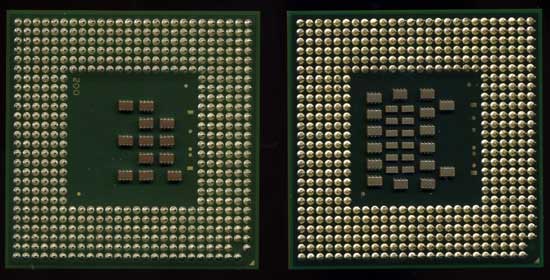
As we mentioned in the first article, the Core Duo (and Solo) processors are not pin-compatible with the older Pentium M, even though they physically have the same number of pins.
When Yonah first started appearing on roadmaps, we knew it as Jonah, which then starting being written as Yonah. Eventually, Intel confirmed its existence and we had always assumed that it would continue to use the name Pentium M. However, given the great importance of the launch of Intel's first dual-core, low power, notebook processor, it shouldn't be much of a surprise that Intel has a new name in store for it. As you've probably already heard, Yonah will receive the marketing name "Core" with the words "Duo" or "Solo" following it depending on whether it is the dual or single core version. The name Centrino will still be there, but instead of referring to the processor as a Pentium M, it'll be called a Core Duo or a Core Solo. The Centrino platform itself will be referred to as Centrino Duo when paired with a Core Duo processor. We have to admit, we kind of like the new name.
Not so pleasant, however, are the new processor numbers that go along with the new processor names. Gone are Intel's simple three-digit numbers and they have since been replaced with a four-digit number preceded by a letter. The letter indicates the thermal envelope of the processor, while the following four digits denote the performance level of the CPU. If you think that this sounds oddly similar to AMD's Turion processor nomenclature, don't worry; you'd be completely right (of course, the Turion only uses two numbers, while Core Duo uses four). Maybe, one of these days, Intel will get around to copying some more important elements of AMD's history, such as an on-die memory controller or at least a serial bus interface.
As an example of the numbers in use, the 2.0GHz processor that we previewed in the first article will be sold under the name "Intel Core Duo T2500". For your reference, the T2600 will run at 2.16GHz (compared to the 2.0GHz T2500). The Core Solo processors will feature a "1" after the "T" denoting a single core; for example, the Intel Core Solo T1300 will run at 1.66GHz.
Intel's Core Duo and Solo processors both support a 667MHz FSB, which is enabled by the 945 chipset that Intel is pairing with them. The move to a 667MHz FSB is necessary, thanks to the increased bandwidth demands of a dual core processor.
As we mentioned in the first article, the Core Duo (and Solo) processors are not pin-compatible with the older Pentium M, even though they physically have the same number of pins.
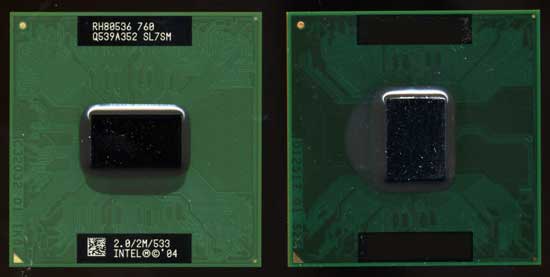
Dothan (Pentium M) on the left, Yonah (Core Duo) on the Right
Dothan (Pentium M) on the left, Yonah (Core Duo) on the Right


103 Comments
View All Comments
Furen - Monday, December 19, 2005 - link
Well, the memory controller is the major difference between the K7 and the K8 but if you compare performance between the two the K8 performs much better. This means that the memory controller directly lead to this increase of performance.In truth the K8's performance is a combination of its micro-architecture and the low-latency access to the memory but since the microarchitecture came first (and was insanely bottlenecked by FSB at higher clocks) the one improvement that lead to the performance difference between the K7 and the K8 was the memory controller. In fact when AMD launched its K8 it said that there would be a 20-30% performance improvement because of the on-die memory controller.
tfranzese - Monday, December 19, 2005 - link
The K8 saw a new instruction set, a slightly lengthened pipeline, SSE2 extensions, SSE3 extensions (eventually), dual-core/multi-cpu design strategies, etc. Oh, and it got an on-die memory controller among other architectural tweaks.I don't think it's valid to attribute so many factors that could have benefitted the architecture to just the memory controller. A lot of small differences add up to a lot.
Furen - Monday, December 19, 2005 - link
Longer pipelines lead to lower performance, the "dual-core design strategies" have nothing to do with a single-core K8's performance benefits over a K7, SSE3 is useless even now and, of course, AMD64 does not benefit 32-bit execution. The only thing that you mentioned that makes a difference is SSE2 and it doesn't really make as much of a difference on A64s as it does on P4s since SIMD vector instructions require multiple passes on the A64. The deeper buffers help, as do the increased L2 cache bandwidth and the increase in L2, but the biggest benefit does come from the integrated memory controller. Cutting access latency is insanely important but having a faster frontside bus (the bus that connects the execution core/cache to the memory controller) is probably what makes A64s perform how they perform.fitten - Tuesday, December 20, 2005 - link
This is not always the case. On branchy code, it is typically true. On non-branchy code, longer pipelines can be very efficient. The problem is that typical codes on the x86 are very branchy so longer pipelines aren't that good on typical x86 codes.
As far as latency numbers and the like, you should do the math to understand why the latency helps. For large cache sizes (512M and larger), the L2 should get above 96% hit rate typically. For 1M L2, hit rates should be 98% or more. Obviously, the application you have will govern these hit rates but this is for "typical" codes. Some applications will see almost no benefit from having an L2 cache at all, for example. The latency of the main memory accesses are felt in the misses (that other 4% or 2%). If the L1 is pretty good (1 cycle penalty), you can zero that out for the calculation. Use some numbers on L2 and main memory access times to get an idea of how it really helps.
So many people just chant "integrated memory controller" as some kind of mantra without even knowing how much it *really* effects memory access times.
Furen - Tuesday, December 20, 2005 - link
Longer pipelines do not help non-branchy code, higher clock speeds do. Longer pipelines allow you to raise clock speeds but if you compare two equally clocked CPUs with similar architectures but different pipeline lenghts then the longer-pipelined one will ALWAYS be slower, since both will eventually mispredict a branch and the penalty on the longer-pipelined one will take a greater hit. In the case of the K8 compared to the K7, however, the branch predictor was improved, the TLBs increased and so on, so you probably end up having the same performance per clock."Typical" code is code that operates on very small data sets, like a word processor. This is not what I'm talking about, however, I'm referring to code that handles massive data sets that cannot fit inside the L2 cache. These include games and streaming media. A K7 performs pretty much the same as a K8 (clock for clock) in office applications and the like, but once you have data traveling down the frontside bus (the K8s frontside bus equivalent is the link between the execution core and the memory controller, which runs at CPU clock) then the performance differences are massive. It may be true that most of the code we execute on a PC does not even touch the main memory to a significant degree but it is also true that we perceive the times when it does as a massive drop in performance. Saying that memory bandwidth (and latency, as the two are directly related) is useless is like saying that a P3 is enough for everyone.
fitten - Wednesday, December 21, 2005 - link
Yes... and longer pipelines is one of the design parameters to achieve higher clock speeds.
Yes, which is why I used "typical" there with a caveat that some workflows do not match that pattern. The math that I mentioned is not difficult to do and the percentages for hit/miss are simply parameters into the equation. You can take any instruction mix and data access pattern, analyze it, and plug the newly found percentages into the equation for a comparison. And... I never said that memory bandwidth is useless. However, I would be inclined into discussion about your bandwidth and latency being directly related (in the general form). Quite obviously, satellite communication has high bandwidth and it is equally obvious that satellite communication has a very high latency, for example.
So, your post confirms exactly what I have said and that AnandTech's benchmarks show (and the conclusions stated in the article). For the majority of applications, since data locality is high, the IMC doesn't do all that much (simply because it isn't used that much). For applications such as games and other applications with data access patterns that do not have a high degree of data locality, the IMC starts to shine. I would also argue that streaming does not fall into that category unless you have poorly optimized code. Intelligent use of prefetching, for example, can hide most of the latency penalties of main memory. I guess we could discuss what "majority of things" means and whether or not games fall into that category. ;)
Furen - Thursday, December 22, 2005 - link
[quote] Yes... and longer pipelines is one of the design parameters to achieve higher clock speeds. [/quote]That's exactly what i said in the line that followed what you quoted. When I said that longer pipelines themselves dont help performance I meant that the clock-for-clock performance benefits of the K8 over the K7 can be mostly attributed to its on-die memory controller. Of course the bigger caches help, as do SSE2 and the other improvements, but the lion's share of the improvement comes from the integrated northbridge (the FSB was a horrible choke point in the K7).
[quote] I would be inclined into discussion about your bandwidth and latency being directly related (in the general form). Quite obviously, satellite communication has high bandwidth and it is equally obvious that satellite communication has a very high latency, for example. [/quote]
Sorry, let me clarify that a bit. When dealing with DRAM (at a set frequency) in a computer system the usable memory bandwidth is directly related the latency. It is not directly proportional but a higher latency will mean a lower usable bandwidth. This is because the memory subsystem in a PC is not just a data transport mechanism but also functions as a data storage array, which gives latency more importance (Satellite communication, on the other hand, only moves data from point to point, it does not store it or modify it in any way, it's just a conduit, which makes its bandwidth somewhat independent of the latency). Now, remember that I'm talking about usable memory bandwidth, not peak bandwidth (which is what manufacturers love to quote). Peak bandwidth is pretty much unrealizable when doing anything useful.
Anyway, I agree with you on the caches, I wanted to point out that the pipeline length itself provides no performance improvements whatsoever, and wanted to say that an integrated memory controller is a wonderful thing. Now, I say that an IMC is wonderful but it does have huge drawbacks, the main one being what AMD is currently dealing with, having to change sockets in order to update memory technology. The thing is, Intel needs flexibility because it is always updating to the newest technologies out there but AMD, on the other hand, actually gained control over the part of the traditional northbridge that affects performance the most without having to go all out and design its own chipsets like Intel does, which is why pretty much all AMD chipsets perform very similarly.
Furen - Thursday, December 22, 2005 - link
Now, can someone tell me how to make decent looking quotes?!!Xenoterranos - Tuesday, December 20, 2005 - link
Considering that bus was developed with dual core and multi-cpu design in thought, I'd say that "dual-core design strategies" had a lot to do with the increase in performance of K8 oer K7. AMD's technical director said something to that effect in so many words in an interview here a few years back; he said they'd built K8 from the ground up for dual core, multi-cpu applications.blackbrrd - Monday, December 19, 2005 - link
Actually, last time I checked, AMDs FPU (since K7) has had 3 execution units, while Intels has had 2 execution units (since pentium..2, or the original pentium, can't remember).