Investigations into Socket 939 Athlon 64 Overclocking
by Jarred Walton on October 3, 2005 4:35 PM EST- Posted in
- CPUs
RAM BIOS Settings
The final area that will need attention with overclocking is the RAM. The type of RAM used will dictate the approach to overclocking that RAM.
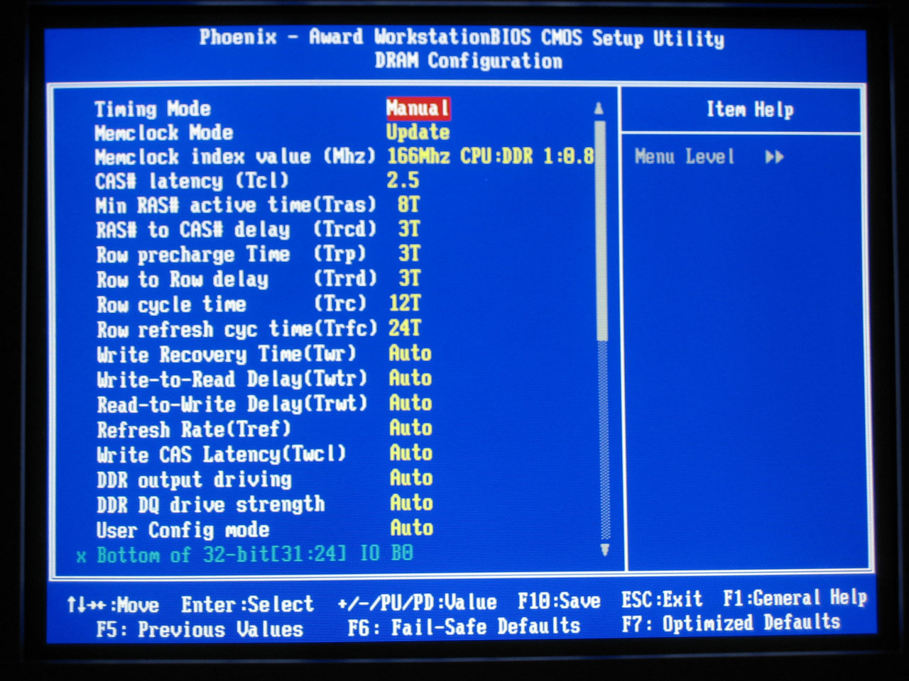
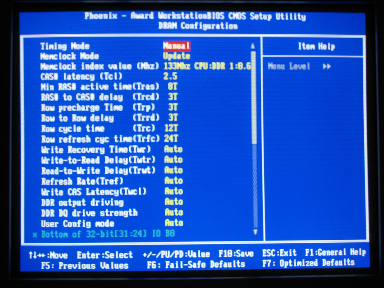
Even if you select the slowest possible timings, some DIMMs won't be able to run much above DDR400 speeds. Value RAM in particular is often what is left after all the high speed blanks are binned out, which is why it can be as cheap as half the cost of quality RAM. The above BIOS screens show our settings for 9x300 with the value and performance RAM - you can see that we had to drop to DDR266 vs. DDR333, since not even the OCZ ran optimally at DDR600. (At least, that's what we needed on this particular board with this particular set of DIMMs. 3-4-4-8 with 2T command rate worked, but was slower than DDR333 2.5-3-3-8 with 1T.) If you're going for top performance, value RAM is a poor choice. If, on the other hand, you want to save money, $85 RAM is a lot more attractive than $150+ RAM. The trick to using value RAM is that you basically have to keep it at or below DDR400 speeds, and this is accomplished by the use of memory ratios. There's a stigma against using higher memory ratios, because it "negates the performance gain." That can be true on some platforms, but it doesn't seem to affect Athlon 64 quite as much due to the integrated memory controller. Let's talk about why.
On the P4 chipsets, the NB talks to the CPU at one speed, and it can talk to RAM at a slower or faster speed. If it talks to RAM faster than it talks to the CPU (i.e. DDR2-533 or DDR2-667 with FSB800), there will be fewer "empty trains" going to the CPU. If it talks slower to the RAM than the FSB, however, there will be more empty slots on the FSB. When we look at Pentium overclocking in the future, we'll cover this more, but the basic idea is that you want the RAM to run at FSB speed or faster if at all possible. Dropping even to DDR333 (which is actually DDR320 for most Intel chipsets) can cause a 5 to 10% performance loss, and DDR266 would be even worse. So, why is Athlon 64 different?
An interesting corollary to the above discussion is in the Northbridge link of AMD vs. Intel. On AMD, the Northbridge is connected via the HyperTransport link. Running at 1000 MHz base (double-pumped makes it equivalent to 2000 MHz), the HT bus is 16-bits wide (2 bytes) with dedicated upstream and downstream links. All told, that gives:
The net result is that while a lower RAM clock speed can still impact performance on Athlon 64 systems, it will not do so as much as on a P4 style configuration. That's the theory, anyway, and we hope to support it with results from several planned overclocking articles.
To illustrate the above points, we've created a brief list of cycle rates and timings of RAM. We'll start with some common RAM speeds, but the actual speed of your RAM will depend on the CPU multiplier and CPU bus speed, among other things. With the clock speeds and timings, we can also calculate the latency and estimate the total memory latency. Remember that the RAM timings are relative to the base bus speed, not the doubled speed, so DDR400 has a 200MHz base clock speed. There is also latency involved internally in the CPU (typically at least a single RAM cycle each way is spent in the memory controller), as well as in sending the address request across the memory bus and receiving the data back across the bus to the CPU (we guessed at two RAM cycles each way). Command rate adds another cycle, and maybe we're wrong or missed some other potential delays.
Everything takes time, and the memory timings generally only reflect the delays caused internally by the RAM. Different clock speeds and timings should produce a different total latency, and we estimate the total memory subsystem latency below. We'll check the actual latency in our benchmarks later. In practice, going from DDR200 to DDR400 RAM will not cut the RAM latency in half, even at the same timings. For reference, our estimated latency is calculated as:
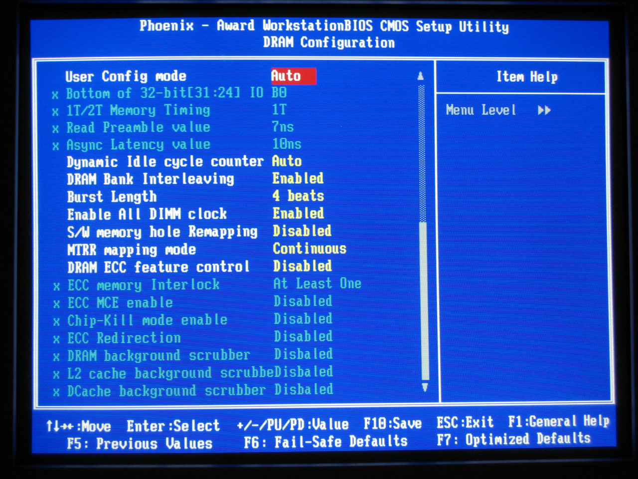
Even with all this information, we haven't even come close to touching on every BIOS option or memory timing that's available. That is, simply put, beyond the scope of this article. There are over a dozen memory timings listed in the DFI BIOS, and we left the majority of them set to Auto. The only items that we changed are CAS, tRCD, tRP, tRAS, and CMD. We may try to look at the other options in the future, but most of the extra settings are not available on the majority of the motherboards, and we want the information contained in this OC Guide to be applicable to more than just the "elite" motherboards.
The final area that will need attention with overclocking is the RAM. The type of RAM used will dictate the approach to overclocking that RAM.
Click to enlarge.
 |
 |
| Click to enlarge. | |
Even if you select the slowest possible timings, some DIMMs won't be able to run much above DDR400 speeds. Value RAM in particular is often what is left after all the high speed blanks are binned out, which is why it can be as cheap as half the cost of quality RAM. The above BIOS screens show our settings for 9x300 with the value and performance RAM - you can see that we had to drop to DDR266 vs. DDR333, since not even the OCZ ran optimally at DDR600. (At least, that's what we needed on this particular board with this particular set of DIMMs. 3-4-4-8 with 2T command rate worked, but was slower than DDR333 2.5-3-3-8 with 1T.) If you're going for top performance, value RAM is a poor choice. If, on the other hand, you want to save money, $85 RAM is a lot more attractive than $150+ RAM. The trick to using value RAM is that you basically have to keep it at or below DDR400 speeds, and this is accomplished by the use of memory ratios. There's a stigma against using higher memory ratios, because it "negates the performance gain." That can be true on some platforms, but it doesn't seem to affect Athlon 64 quite as much due to the integrated memory controller. Let's talk about why.
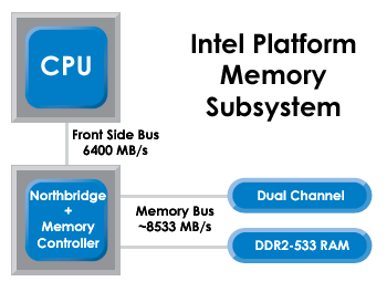
On the P4 chipsets, the NB talks to the CPU at one speed, and it can talk to RAM at a slower or faster speed. If it talks to RAM faster than it talks to the CPU (i.e. DDR2-533 or DDR2-667 with FSB800), there will be fewer "empty trains" going to the CPU. If it talks slower to the RAM than the FSB, however, there will be more empty slots on the FSB. When we look at Pentium overclocking in the future, we'll cover this more, but the basic idea is that you want the RAM to run at FSB speed or faster if at all possible. Dropping even to DDR333 (which is actually DDR320 for most Intel chipsets) can cause a 5 to 10% performance loss, and DDR266 would be even worse. So, why is Athlon 64 different?
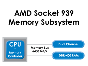
An interesting corollary to the above discussion is in the Northbridge link of AMD vs. Intel. On AMD, the Northbridge is connected via the HyperTransport link. Running at 1000 MHz base (double-pumped makes it equivalent to 2000 MHz), the HT bus is 16-bits wide (2 bytes) with dedicated upstream and downstream links. All told, that gives:
2000 MHz * 2 bytes = 4000 MB/sThe total HT bandwidth is thus 8000 MB/s - 4000 MB/s in each direction. Here's the catch, though: this bandwidth is separate from the memory bandwidth. If you've ever tried overclocking the HT bus speed and found the results to be of little help, performance-wise, that should hopefully clear things up. There is rarely (if ever) 4 GB/s of data in either direction between the CPU and Northbridge. It's like putting an eight-lane highway through a rural farming community; since there's very little traffic to begin with, the extra lanes (bandwidth) won't help much. That's not to say this is a poor design decision - better to have too much available bandwidth than not enough! The P4 design doesn't suffer from a lack of bandwidth either; the problem is that the time in which it takes to get data from the RAM to the CPU is quite a bit longer - in other words, higher latencies.
The net result is that while a lower RAM clock speed can still impact performance on Athlon 64 systems, it will not do so as much as on a P4 style configuration. That's the theory, anyway, and we hope to support it with results from several planned overclocking articles.
To illustrate the above points, we've created a brief list of cycle rates and timings of RAM. We'll start with some common RAM speeds, but the actual speed of your RAM will depend on the CPU multiplier and CPU bus speed, among other things. With the clock speeds and timings, we can also calculate the latency and estimate the total memory latency. Remember that the RAM timings are relative to the base bus speed, not the doubled speed, so DDR400 has a 200MHz base clock speed. There is also latency involved internally in the CPU (typically at least a single RAM cycle each way is spent in the memory controller), as well as in sending the address request across the memory bus and receiving the data back across the bus to the CPU (we guessed at two RAM cycles each way). Command rate adds another cycle, and maybe we're wrong or missed some other potential delays.
Everything takes time, and the memory timings generally only reflect the delays caused internally by the RAM. Different clock speeds and timings should produce a different total latency, and we estimate the total memory subsystem latency below. We'll check the actual latency in our benchmarks later. In practice, going from DDR200 to DDR400 RAM will not cut the RAM latency in half, even at the same timings. For reference, our estimated latency is calculated as:
7 * (Cycle Latency) + CL + 0.1 * tRCD + 0.05 * tRPIt would be different for other platforms, and it's probably off by as much as 20%, we'd guess. The "7" represents the command rate, CPU to memory controller delays, and memory controller to RAM delays. We did use some tests to try to come up with a good estimate, but take the estimated latency in the following table with a serious dose of skepticism. For a P4 platform, the major change is that the inclusion of the NB will change the "7" factor to something much larger - perhaps 14 to 20. (We'll look at that in a future article.)
| RAM Speeds; Timings and Theoretical Latencies | |||||||||||
| RAM Rating | Base Speed | ns per cycle | CAS | tRCD | tRP | tRAS | CL ns | tRCD ns | tRP ns | tRAS ns | Estimated Latency |
| DDR266 | 133.33 | 7.5 | 2 | 2 | 2 | 5 | 15 | 15 | 15 | 37.5 | 69.75 |
| DDR266 | 133.33 | 7.5 | 2.5 | 3 | 3 | 7 | 18.75 | 22.5 | 22.5 | 52.5 | 74.63 |
| DDR266 | 133.33 | 7.5 | 3 | 4 | 4 | 8 | 22.5 | 30 | 30 | 60 | 79.5 |
| DDR333 | 166.67 | 6 | 2 | 2 | 2 | 5 | 12 | 12 | 12 | 30 | 55.8 |
| DDR333 | 166.67 | 6 | 2.5 | 3 | 3 | 7 | 15 | 18 | 18 | 42 | 59.7 |
| DDR333 | 166.67 | 6 | 3 | 4 | 4 | 8 | 18 | 24 | 24 | 48 | 63.6 |
| DDR400 | 200 | 5 | 2 | 2 | 2 | 5 | 10 | 10 | 10 | 25 | 46.5 |
| DDR400 | 200 | 5 | 2.5 | 3 | 3 | 7 | 12.5 | 15 | 15 | 35 | 49.75 |
| DDR400 | 200 | 5 | 3 | 4 | 4 | 8 | 15 | 20 | 20 | 40 | 53 |
| DDR450 | 225 | 4.44 | 2 | 2 | 2 | 5 | 8.89 | 8.89 | 8.89 | 22.22 | 41.33 |
| DDR450 | 225 | 4.44 | 2.5 | 3 | 3 | 7 | 11.11 | 13.33 | 13.33 | 31.11 | 44.22 |
| DDR450 | 225 | 4.44 | 3 | 4 | 4 | 8 | 13.33 | 17.78 | 17.78 | 35.56 | 47.11 |
| DDR500 | 250 | 4 | 2 | 2 | 2 | 5 | 8 | 8 | 8 | 20 | 37.2 |
| DDR500 | 250 | 4 | 2.5 | 3 | 3 | 7 | 10 | 12 | 12 | 28 | 39.8 |
| DDR500 | 250 | 4 | 3 | 4 | 4 | 8 | 12 | 16 | 16 | 32 | 42.4 |
Even with all this information, we haven't even come close to touching on every BIOS option or memory timing that's available. That is, simply put, beyond the scope of this article. There are over a dozen memory timings listed in the DFI BIOS, and we left the majority of them set to Auto. The only items that we changed are CAS, tRCD, tRP, tRAS, and CMD. We may try to look at the other options in the future, but most of the extra settings are not available on the majority of the motherboards, and we want the information contained in this OC Guide to be applicable to more than just the "elite" motherboards.


101 Comments
View All Comments
Deathcharge - Saturday, October 15, 2005 - link
also what do you think of opteron 144 or 146? the 144 are very cheap and they OC quite well apprentlypmorcos - Thursday, October 13, 2005 - link
Before I comment, you should know that I have been overclocking for 8 years now and literally overclocked all but one of the chips you mentioned in the beginning of this very good article. The HT multiplier was new to me with my most recent DFI NF4-SLI-DR board so I found that extremely useful and plan to see if I can up my speeds...but I digress.I think it would be extremely valuable to TRY to put in words the order with which an overclocker should approach making changes to settings. In other words, which is likely to be the most limiting/critical aspect(s) and from there tweak the others to max the system out.
It would be interesting to say, for example, that you start with a "safe" power settings (which is pretty obviously the limiting factor). For example, let's say your CPU and memory are rated at 1.3 and 2.8 V respectively. Why not go straight to "safe" settings for the two and tweak from there? It seems that the most useful piece of information that is NOT provided by anandtech or anyone else for that matter is a voltage and temp graph of stability/viability for these chips. It would be simple to take 3 samples (at a cost) of each chip and run the test with "average" cooling and find out what is "safe". For example if running all stock settings but upping voltages to say 2.4/3.6 V in the example above, you might see stability up to 1.65 / 3.1 V with the parts catching fire at say 1.8/3.3 V or stable at temp readings for cpu/memory of 44/47C but unstable above that. Once armed with these two graphs of information averaged from 3 chips tested the rest is very straight forward.
You simply set the cpu volts to 1.65 and memory to 3.1 V (the safe settings; check real voltages vis bios monitoring) and now you up your fsb and tweak your memory timings and in a few minutes you are running max.
Why do I think this is more valuable that showing us a graph of your results? Because like many I'm squeemish about upping the voltage on my processor and memory. I'm worried much more about the power-on affects than I am the "long-term" effects.
In computers, there are no long-terms for an overclocker. An overclocker's comp is 60% hardware and 40% software. Their greatest joy is in posting results on their favorite forum. I want to know that when I hit the power button...that the 1.7V setting does NOT have a 10% chance of blowing my processor.
My ramblings. Thanks again for another great article from by far the VERY BEST place in the world to find out how computer parts work.
JarredWalton - Thursday, October 13, 2005 - link
Thanks pmorcos.I'm working on the X2 3800+ OC followup, and I've gone back and done further testing of temperatures and voltages. Chips differ, so the real advice I have on that subject is to test your own chip extensively. I've heard of people doing 2.8 GHz on 1.500V with the Venice chips, but mine won't even POST at those settings. I think 1.65 or 1.70V was required to POST, and even then I couldn't run stable benchmarks without more voltage.
I will also be trying to cover a bit more of the "how to" process in the next one. Consider this the foundation, and the next article will refine the approach a bit. Your comments on what you'd like to see more of are definitely welcome, though, and I'll try to address the order and approach I take next.
Concerning another comment: "I want to know that when I hit the power button...that the 1.7V setting does NOT have a 10% chance of blowing my processor." I'm not quite sure I understand the concern or know how to test that. Are you saying that the power on process has more voltage fluctuations and may therefore toast the CPU in the first second? (I haven't had that happen over the past several months of testing this chip and others in overclocked setups.) I must admit that I'm extremely nervous about the 1.850V I used for running at 2.80 GHz, but even then the chip continued to function (for now - heheh).
Cheers!
Jarred Walton
WhipperSnapper - Thursday, October 13, 2005 - link
That was one of the best computer enthusiast website articles that I've read in a long time, but perhaps I don't get around too much. I'd like to hear more about the problems that spilled over to other components, such as the SATA hard drive (mentioned in the Final Thoughts) and whether or not the overclocking can be isolated to the CPU and RAM. I also wondered if there was a reason why you guys used a SATA hard drive and not an IDE drive and whether overclocking requires a SATA hard drive. (I don't see why it would.)
Also, have you guys tried to do any tests using memory stick heatsinks? Do they actually do anything? That subject might make for a worthwhile article on its own--RAM cooling.
aptinio - Saturday, October 8, 2005 - link
bravo! great article. very informative but not too bloated. can't wait to finally upgrade my amd k6-II with 1mb l3 cache on the motherboard! lol!Kougar7 - Thursday, October 6, 2005 - link
Thank you for the excellent, comprehensive, and very thorough article! :-) It must have taken a massive amount of work and time to complete. It’s answered my recent musings about my own Crucial value ram, which looks much nicer now! It’s also solved a question about OCing with recent AMD 64 chips, amongst also correcting a few personal misconceptions I’ve had.I just wish to ask if you plan to include a similar article on OCing with P4s? I personally run a 2.8C (Northwood) @ 3.4 rock solid at the 3.4C’s default voltage, but am now wondering exactly what performance hits, if any, that I’ve taken from having to use a 5:4 CPU:DRAM ratio instead of the previous 1:1, even though I’ve kept it at DDR390 and the timings better than specs.
I’m planning to bench the differences from a 1:1 ratio, a 3:2 ratio at highest speed I can get (sub-DDR333), my current setup, and finally one other setting where I got the value memory to run 2-2-2-6 timings, to get a more solid idea on which performs best with some solid figures.
Although the core and the platform itself both have both changed, I’d still be interested in a Intel processor based test! Perhaps instead of a P4, maybe a Pentium “D” OCing article similar to what you have planned with the X2 3800+? ;-)
I’m very much looking forward to your X2 3800+ OCing review!! You rock :-D Thanks in advance for it!
JarredWalton - Thursday, October 6, 2005 - link
I'm trying to get a socket 775 motherboard that will overclock well with Pentium D 820. Once I get that, I can give it a go. I've also got a Pentium 4 505 and a 540 that I want to run some similar tests on. First, though, I need an appropriate motherboard.clue22 - Thursday, October 6, 2005 - link
so basically what the everybody is saying about the value RAM vs. low latency more expensive RAM is that for the athlon 64 it is basically a waste of money (i.e. you only get about 5% performance gain), but usually spend 100% or more money to get the "better" RAM. i have to build a couple of systems pretty soon and now i believe that my money would be better spent on 2GB of value RAM vs. 1GB of the more expensive stuff. does anyone know of a test that has been run with 2.5-3-3-8-1t vs. 2-2-2-5-1t? also why does every mid-range/gaming/hot-rod price guide ever recommend the either the samsung tccd (or tcc5) or winbond bh5/ch5 based memory if it has so little effect on performance. finally is it even important anymore (if it ever was) to get matched pairs of memory that are bundled together (supposedly manufactured at the same time)? i was looking at some corsair (had good experience with them in the past) xms3200xl RAM but now i think i should get more of their value select memory instead.thanks
RupertS - Wednesday, October 26, 2005 - link
so basically what the everybody is saying about the value RAM vs. low latency more expensive RAM is that for the athlon 64 it is basically a waste of moneyThis may not be a general rule.
It may just be that at this stage of development for GPU's, CPU's and memory, memory has more than enough capacity - it is not the choke point. If GPU and CPU speed were to improve while memory speed stayed the same, you might reach the point where increasing GPU and CPU speed was non-productive for games, while overclocking memory provided large performance improvements.
rabbit fighter - Wednesday, October 5, 2005 - link
Where was this explained? He said the 3200 was better in the first paragraph and that he would explain later, but I can't find the later explanation!