Investigations into Socket 939 Athlon 64 Overclocking
by Jarred Walton on October 3, 2005 4:35 PM EST- Posted in
- CPUs
DFI nF4 Infinity
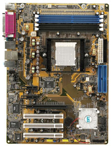
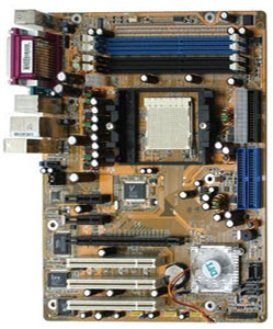
We wanted to spend a few minutes looking at the motherboard options before continuing - a mini review if you will, as we haven't officially reviewed this board and we want to compare it to the LANPARTY UT nF4 Ultra-D. We're using the DFI NF4 INFINITY, but it is actually just the new name for the DFI NF4-DAGF. There are multiple models of the INFINITY/DAGF, using everything from the base nForce4 4X chipset to the top nForce4 Ultra and SLI. We're using the "middle" model, the nForce4 Standard. The main difference is that all the networking features of the chipset are enabled and official support for 1000 MHz HyperTransport is also present. The only extra that the Ultra offers is SATA-II (3 Gbps) hard drive support, while the 4X limits the HT bus to 800 MHz. SLI adds dual PEG slots to the mix, of course. We heard directly from DFI that the DAGF was being renamed to "INFINITY", but if you still think that there's a difference, we offer these two shots obtained from Newegg and TigerDirect.
TigerDirect lists the board as the INFINITY while Newegg uses the older DAGF moniker. We've resized the images for comparison, with TigerDirect on the left and Newegg on the right. Other than a slight difference in contrast levels and viewing angle, we can't spot any changes. Besides, we're inclined to take DFI at their word. Here's a better shot of our particular board.
Unlike the LanParty series, the Infinity is pretty boring in terms of looks. A standard brownish PCB with no UV reactive parts isn't the best fit for a windowed case, but if you're like me and don't care for case windows, it doesn't really matter. Also missing relative to the LanParty are the rounded cables and onboard power and reset buttons. Those buttons can be handy for testing outside of a case. (Of course, if you're adventurous, you can always just use a small metal item to short the required pins to accomplish the same result - don't blame us if you fry your system that way, though!) One complaint that we did have was with the X16 PEG retention mechanism. Many boards have a clip that locks the rear of the graphics card into place, but the Infinity has a sort of "hook" design. It works okay for holding the GPU in the slot, but removing the GPU can be a bit more difficult than what we'd like. We'd also prefer a larger heat sink on the Northbridge, perhaps with passive cooling. The NB did get quite warm at the highest overclocks, and there looks to be plenty of room to move it up closer to the CPU socket. The small fan did make a bit of noise, though "silent" and "overclocking" rarely go together.
The feature list of the board is very similar to the LanParty boards. The BIOS offers very good tweaking options, but voltages are slightly more limited than the higher-end boards. 3.2V maximum on the RAM is plenty for most people, but it did prove limiting on some OCZ VX Gold that we tried, reaching a maximum of 2-3-3-8-1T timings at DDR500. (That RAM was not used during testing for this particular article, so we mention it merely as a point of interest.) The CPU voltage topped out a 1.85V, which is a lot higher than the default voltage of most 90nm AMD chips. We're a little uncomfortable pushing our CPUs even to that level, though with water cooling or something more exotic, a higher voltage level might prove useful.
Overall, we're very impressed with this value offering from DFI. They basically stripped away the flash and the frills and knocked around $20 off the price of the LanParty UT nF4 Ultra-D. The question is: do you really want to save the $20? Modders can try turning the Ultra-D board into an SLI model, and the rounded cables and UT reactive design may appeal to some. On the other hand, the Infinity SLI guarantees SLI capability and costs about the same amount as the Ultra-D. If you want to push overclocking a little further, the LanParty boards (and competitors) might be a bit better. If you're trying to stick to a budget without cutting necessary features, the Infinity line keeps you covered.
Having selected the processor and motherboard, we're still only half way through our critical component choices. Hard drives, floppy drives, optical drives, and even graphics cards have little to no impact on overclocking, so you can get whatever you want in those areas. We'd question the purchase of a low end graphics card with such a system, unless there's a specific desire to have a fast processor for video/audio encoding. That sort of work is often for a real job, though, and we're hesitant to suggest that anyone overclock a system that is being used for important work. If a gaming PC crashes and somehow corrupts your entire hard drive, you reformat and reinstall. A work PC going through the same problems would be a lot more painful. We've already given our warnings about overclocking, however, so do what you will. What remains, then, are the last three components that will generally have an impact on your overclocking endeavors.
We wanted to spend a few minutes looking at the motherboard options before continuing - a mini review if you will, as we haven't officially reviewed this board and we want to compare it to the LANPARTY UT nF4 Ultra-D. We're using the DFI NF4 INFINITY, but it is actually just the new name for the DFI NF4-DAGF. There are multiple models of the INFINITY/DAGF, using everything from the base nForce4 4X chipset to the top nForce4 Ultra and SLI. We're using the "middle" model, the nForce4 Standard. The main difference is that all the networking features of the chipset are enabled and official support for 1000 MHz HyperTransport is also present. The only extra that the Ultra offers is SATA-II (3 Gbps) hard drive support, while the 4X limits the HT bus to 800 MHz. SLI adds dual PEG slots to the mix, of course. We heard directly from DFI that the DAGF was being renamed to "INFINITY", but if you still think that there's a difference, we offer these two shots obtained from Newegg and TigerDirect.
 |
 |
TigerDirect lists the board as the INFINITY while Newegg uses the older DAGF moniker. We've resized the images for comparison, with TigerDirect on the left and Newegg on the right. Other than a slight difference in contrast levels and viewing angle, we can't spot any changes. Besides, we're inclined to take DFI at their word. Here's a better shot of our particular board.
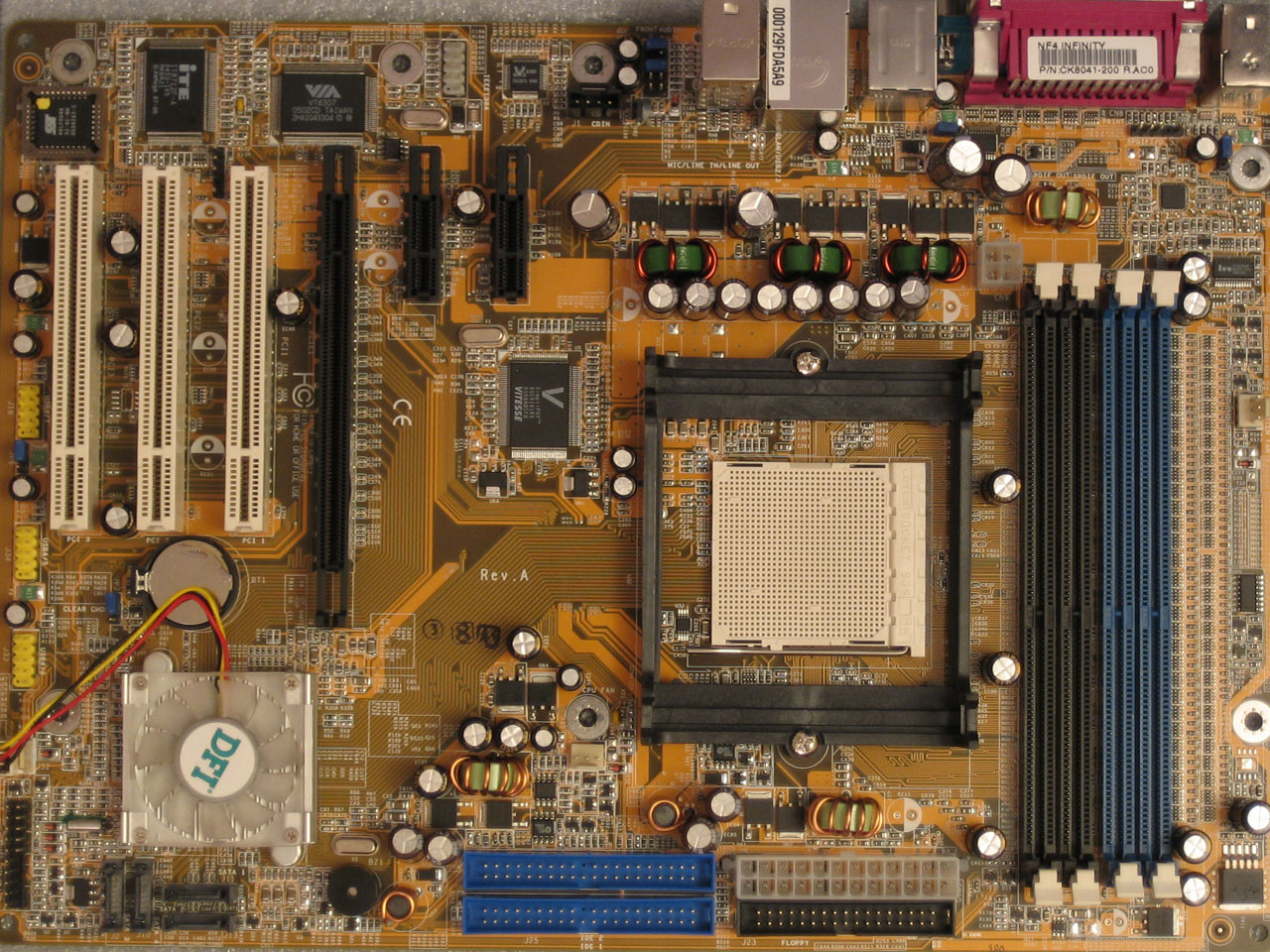
Click to enlarge.
Unlike the LanParty series, the Infinity is pretty boring in terms of looks. A standard brownish PCB with no UV reactive parts isn't the best fit for a windowed case, but if you're like me and don't care for case windows, it doesn't really matter. Also missing relative to the LanParty are the rounded cables and onboard power and reset buttons. Those buttons can be handy for testing outside of a case. (Of course, if you're adventurous, you can always just use a small metal item to short the required pins to accomplish the same result - don't blame us if you fry your system that way, though!) One complaint that we did have was with the X16 PEG retention mechanism. Many boards have a clip that locks the rear of the graphics card into place, but the Infinity has a sort of "hook" design. It works okay for holding the GPU in the slot, but removing the GPU can be a bit more difficult than what we'd like. We'd also prefer a larger heat sink on the Northbridge, perhaps with passive cooling. The NB did get quite warm at the highest overclocks, and there looks to be plenty of room to move it up closer to the CPU socket. The small fan did make a bit of noise, though "silent" and "overclocking" rarely go together.
| DFI nF4 Infinity Specifications | |
| CPU Interface | Socket 939 Athlon 64 |
| Chipset | nForce4 Standard (single chip) |
| BUS Speeds | 200MHz to 450MHz (in 1MHz increments) |
| PCI/AGP Speeds | Asynchronous (Fixed) |
| PCI Express | 100MHz to 145MHz in 1MHz increments |
| CPU Voltage | Auto, 0.800V to 1.850V in 0.025V increments |
| DRAM Voltage | 2.5V to 3.2V in 0.1V increments |
| Chipset Voltage | 1.5V, 1.6V, 1.7V |
| Hyper Transport Ratios | Auto, 1.0, 2.0, 3.0, 4.0, 5.0 |
| LDT Bus Transfer | 16/16, 16/8, 8/16, 8/8 |
| CPU Ratios | Auto, 4x to 25x in .5x increments |
| DRAM Speeds | Auto, 100, 133, 150, 166, 200 |
| Memory Command Rate | Auto, 1T, 2T |
| Memory Slots | Four 184-pin DDR Dual-Channel Slots Unbuffered ECC or non-ECC Memory to 4GB Total |
| Expansion Slots | 1 X16 PCIe Slots 2 X1 PCIe 3 PCI Slots |
| Onboard SATA | 4-Drive SATA by nF4 |
| Onboard IDE | Two Standard NVIDIA ATA133/100/66 (4 drives) |
| SATA/IDE RAID | 4-Drive SATA plus 4-Drive IDE (8 total) Can be combined in RAID 0, 1 |
| Onboard USB 2.0/IEEE-1394 | 10 USB 2.0 ports supported nF4 2 1394A FireWire ports by VIA VT6307 |
| Onboard LAN | Gigabit Ethernet PCIe by Vitesse VSC8201 PHY |
| Onboard Audio | Realtek ALC655 6-Channel codec 3 UAJ audio jacks CD-in, front audio, and coaxial SPDIF In and Out |
| BIOS | Award 8/11/2005 Release, CK84D811 |
The feature list of the board is very similar to the LanParty boards. The BIOS offers very good tweaking options, but voltages are slightly more limited than the higher-end boards. 3.2V maximum on the RAM is plenty for most people, but it did prove limiting on some OCZ VX Gold that we tried, reaching a maximum of 2-3-3-8-1T timings at DDR500. (That RAM was not used during testing for this particular article, so we mention it merely as a point of interest.) The CPU voltage topped out a 1.85V, which is a lot higher than the default voltage of most 90nm AMD chips. We're a little uncomfortable pushing our CPUs even to that level, though with water cooling or something more exotic, a higher voltage level might prove useful.
Overall, we're very impressed with this value offering from DFI. They basically stripped away the flash and the frills and knocked around $20 off the price of the LanParty UT nF4 Ultra-D. The question is: do you really want to save the $20? Modders can try turning the Ultra-D board into an SLI model, and the rounded cables and UT reactive design may appeal to some. On the other hand, the Infinity SLI guarantees SLI capability and costs about the same amount as the Ultra-D. If you want to push overclocking a little further, the LanParty boards (and competitors) might be a bit better. If you're trying to stick to a budget without cutting necessary features, the Infinity line keeps you covered.
Having selected the processor and motherboard, we're still only half way through our critical component choices. Hard drives, floppy drives, optical drives, and even graphics cards have little to no impact on overclocking, so you can get whatever you want in those areas. We'd question the purchase of a low end graphics card with such a system, unless there's a specific desire to have a fast processor for video/audio encoding. That sort of work is often for a real job, though, and we're hesitant to suggest that anyone overclock a system that is being used for important work. If a gaming PC crashes and somehow corrupts your entire hard drive, you reformat and reinstall. A work PC going through the same problems would be a lot more painful. We've already given our warnings about overclocking, however, so do what you will. What remains, then, are the last three components that will generally have an impact on your overclocking endeavors.


101 Comments
View All Comments
Deathcharge - Saturday, October 15, 2005 - link
also what do you think of opteron 144 or 146? the 144 are very cheap and they OC quite well apprentlypmorcos - Thursday, October 13, 2005 - link
Before I comment, you should know that I have been overclocking for 8 years now and literally overclocked all but one of the chips you mentioned in the beginning of this very good article. The HT multiplier was new to me with my most recent DFI NF4-SLI-DR board so I found that extremely useful and plan to see if I can up my speeds...but I digress.I think it would be extremely valuable to TRY to put in words the order with which an overclocker should approach making changes to settings. In other words, which is likely to be the most limiting/critical aspect(s) and from there tweak the others to max the system out.
It would be interesting to say, for example, that you start with a "safe" power settings (which is pretty obviously the limiting factor). For example, let's say your CPU and memory are rated at 1.3 and 2.8 V respectively. Why not go straight to "safe" settings for the two and tweak from there? It seems that the most useful piece of information that is NOT provided by anandtech or anyone else for that matter is a voltage and temp graph of stability/viability for these chips. It would be simple to take 3 samples (at a cost) of each chip and run the test with "average" cooling and find out what is "safe". For example if running all stock settings but upping voltages to say 2.4/3.6 V in the example above, you might see stability up to 1.65 / 3.1 V with the parts catching fire at say 1.8/3.3 V or stable at temp readings for cpu/memory of 44/47C but unstable above that. Once armed with these two graphs of information averaged from 3 chips tested the rest is very straight forward.
You simply set the cpu volts to 1.65 and memory to 3.1 V (the safe settings; check real voltages vis bios monitoring) and now you up your fsb and tweak your memory timings and in a few minutes you are running max.
Why do I think this is more valuable that showing us a graph of your results? Because like many I'm squeemish about upping the voltage on my processor and memory. I'm worried much more about the power-on affects than I am the "long-term" effects.
In computers, there are no long-terms for an overclocker. An overclocker's comp is 60% hardware and 40% software. Their greatest joy is in posting results on their favorite forum. I want to know that when I hit the power button...that the 1.7V setting does NOT have a 10% chance of blowing my processor.
My ramblings. Thanks again for another great article from by far the VERY BEST place in the world to find out how computer parts work.
JarredWalton - Thursday, October 13, 2005 - link
Thanks pmorcos.I'm working on the X2 3800+ OC followup, and I've gone back and done further testing of temperatures and voltages. Chips differ, so the real advice I have on that subject is to test your own chip extensively. I've heard of people doing 2.8 GHz on 1.500V with the Venice chips, but mine won't even POST at those settings. I think 1.65 or 1.70V was required to POST, and even then I couldn't run stable benchmarks without more voltage.
I will also be trying to cover a bit more of the "how to" process in the next one. Consider this the foundation, and the next article will refine the approach a bit. Your comments on what you'd like to see more of are definitely welcome, though, and I'll try to address the order and approach I take next.
Concerning another comment: "I want to know that when I hit the power button...that the 1.7V setting does NOT have a 10% chance of blowing my processor." I'm not quite sure I understand the concern or know how to test that. Are you saying that the power on process has more voltage fluctuations and may therefore toast the CPU in the first second? (I haven't had that happen over the past several months of testing this chip and others in overclocked setups.) I must admit that I'm extremely nervous about the 1.850V I used for running at 2.80 GHz, but even then the chip continued to function (for now - heheh).
Cheers!
Jarred Walton
WhipperSnapper - Thursday, October 13, 2005 - link
That was one of the best computer enthusiast website articles that I've read in a long time, but perhaps I don't get around too much. I'd like to hear more about the problems that spilled over to other components, such as the SATA hard drive (mentioned in the Final Thoughts) and whether or not the overclocking can be isolated to the CPU and RAM. I also wondered if there was a reason why you guys used a SATA hard drive and not an IDE drive and whether overclocking requires a SATA hard drive. (I don't see why it would.)
Also, have you guys tried to do any tests using memory stick heatsinks? Do they actually do anything? That subject might make for a worthwhile article on its own--RAM cooling.
aptinio - Saturday, October 8, 2005 - link
bravo! great article. very informative but not too bloated. can't wait to finally upgrade my amd k6-II with 1mb l3 cache on the motherboard! lol!Kougar7 - Thursday, October 6, 2005 - link
Thank you for the excellent, comprehensive, and very thorough article! :-) It must have taken a massive amount of work and time to complete. It’s answered my recent musings about my own Crucial value ram, which looks much nicer now! It’s also solved a question about OCing with recent AMD 64 chips, amongst also correcting a few personal misconceptions I’ve had.I just wish to ask if you plan to include a similar article on OCing with P4s? I personally run a 2.8C (Northwood) @ 3.4 rock solid at the 3.4C’s default voltage, but am now wondering exactly what performance hits, if any, that I’ve taken from having to use a 5:4 CPU:DRAM ratio instead of the previous 1:1, even though I’ve kept it at DDR390 and the timings better than specs.
I’m planning to bench the differences from a 1:1 ratio, a 3:2 ratio at highest speed I can get (sub-DDR333), my current setup, and finally one other setting where I got the value memory to run 2-2-2-6 timings, to get a more solid idea on which performs best with some solid figures.
Although the core and the platform itself both have both changed, I’d still be interested in a Intel processor based test! Perhaps instead of a P4, maybe a Pentium “D” OCing article similar to what you have planned with the X2 3800+? ;-)
I’m very much looking forward to your X2 3800+ OCing review!! You rock :-D Thanks in advance for it!
JarredWalton - Thursday, October 6, 2005 - link
I'm trying to get a socket 775 motherboard that will overclock well with Pentium D 820. Once I get that, I can give it a go. I've also got a Pentium 4 505 and a 540 that I want to run some similar tests on. First, though, I need an appropriate motherboard.clue22 - Thursday, October 6, 2005 - link
so basically what the everybody is saying about the value RAM vs. low latency more expensive RAM is that for the athlon 64 it is basically a waste of money (i.e. you only get about 5% performance gain), but usually spend 100% or more money to get the "better" RAM. i have to build a couple of systems pretty soon and now i believe that my money would be better spent on 2GB of value RAM vs. 1GB of the more expensive stuff. does anyone know of a test that has been run with 2.5-3-3-8-1t vs. 2-2-2-5-1t? also why does every mid-range/gaming/hot-rod price guide ever recommend the either the samsung tccd (or tcc5) or winbond bh5/ch5 based memory if it has so little effect on performance. finally is it even important anymore (if it ever was) to get matched pairs of memory that are bundled together (supposedly manufactured at the same time)? i was looking at some corsair (had good experience with them in the past) xms3200xl RAM but now i think i should get more of their value select memory instead.thanks
RupertS - Wednesday, October 26, 2005 - link
so basically what the everybody is saying about the value RAM vs. low latency more expensive RAM is that for the athlon 64 it is basically a waste of moneyThis may not be a general rule.
It may just be that at this stage of development for GPU's, CPU's and memory, memory has more than enough capacity - it is not the choke point. If GPU and CPU speed were to improve while memory speed stayed the same, you might reach the point where increasing GPU and CPU speed was non-productive for games, while overclocking memory provided large performance improvements.
rabbit fighter - Wednesday, October 5, 2005 - link
Where was this explained? He said the 3200 was better in the first paragraph and that he would explain later, but I can't find the later explanation!