Understanding the Cell Microprocessor
by Anand Lal Shimpi on March 17, 2005 12:05 AM EST- Posted in
- CPUs
Manufacturing, Die Size and Clock Speed
Intel's superiority in manufacturing is responsible for the majority of their technological advances in microprocessors over the past decade, and it's often argued that there isn't a company around that could come close to matching Intel's manufacturing abilities - with the exception of IBM.The Cell prototype boasts some pretty major manufacturing specs:
- 90nm SOI manufacturing process
- 221 mm2 die area
- 234M transistors
- > 4GHz observed clock speed
When it was first announced, the chip sounded massive, but its specifications compare extremely well to Intel's upcoming Pentium D processor; let's take a look at its vitals:
Intel Pentium D Processor
- 90nm strained silicon manufacturing process
- 206 mm2 die area
- 230M transistors
- 2.8GHz - 3.2GHz clock speed
With a slightly larger chip and a few million transistors more, Cell is supposed to be able to run at a minimum of 25% higher clock frequency than Intel's forthcoming Pentium D. We'll let that sit in for a moment...
Dynamic Logic
At first glance, a 90nm SOI Cell running at between 3 - 5GHz looks extremely impressive. After all, the fastest 90nm CPU IBM currently produces runs at 2.5GHz, not to mention that even Intel, the king of clock speed, can't mass produce anything faster than 3.8GHz on their 90nm process. But let's dig a little deeper.The Pentium 4 has two ALUs that run at twice its internal clock speed - so in the case of a Pentium 4 660, that means that two of the more frequently used execution units operate at 7.2GHz - on a 90nm process. So, it's possible to get circuits to run at higher clock speeds, even in the 3 - 5GHz range, on current 90nm processes - it just takes a little bit of creative logic design.
It's been confirmed that Cell is using some sort of dynamic logic as opposed to static CMOS in order to control transistor counts and improve operating frequencies. Intel uses a number of specialized logic techniques in their double-pumped ALUs to reach their 7GHz+ operating frequencies, and Intel has discussed techniques that are similar to the dynamic logic used in Cell.
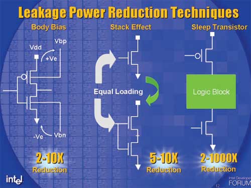
The diagram on the right of a "sleep transistor" should look very familiar by the end of this article
Transistors and You
Just about any AnandTech reader who has followed our CPU articles has heard us count transistors before, but understanding how transistors work is quite critical to understanding how IBM can talk about 3 - 5GHz clock speeds for Cell.We'll spare you the details about how transistors are made and the physics behind them in an attempt to keep this section as brief, but as informative, as possible. It's quite common to refer to a transistor as a "switch" much like a light switch, so how does a transistor function like a switch? Below, we have a representation of a p-type transistor:
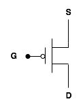
The input to the gate of the p-type transistor is what makes it function as a switch. If you apply the right voltage to the gate, thus making it a logical "1" or high, current doesn't flow in the transistor. If you don't apply any voltage to the gate, current can flow. Just like a light switch, flip it one way and the light turns on; flip it another and you're in the dark.
There's another type of transistor that we'll be talking about here: the n-type transistor:
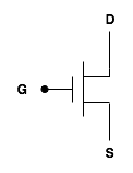
CMOS circuits work by using pairs of n- and p-type transistors (that's where the Complementary element of CMOS comes from). CMOS circuits are by far the most predominant in modern day microprocessors, but as you will soon see, that doesn't mean that they are without flaws.


70 Comments
View All Comments
faboloso112 - Thursday, March 17, 2005 - link
ahh i love bedtime stories!great read...VERY informative!
ksherman - Thursday, March 17, 2005 - link
sweet article! way over my head, but there were some parts that were dropped down to my level of understanding. Leave it to anand to tell the real story. It will be interesting to see how willing some companies will be to accomidate Sony's ratical processor... bu tas long as theirs money... Do you think that it is possible to (down the road) flop a x86 chip in place of the PPE? wouldn't hat make the Cell compatible with the current processing standards?ProviaFan - Thursday, March 17, 2005 - link
Describing this as a "sit down read" type of article makes me want to print it out to put it in the magazine rack, because I don't have a laptop + 802.11g to peruse AnandTech while I'm, er... ;)xsilver - Thursday, March 17, 2005 - link
nice, definitley one of those "sit down reads".... some serious shiznit ;)cosmotic - Thursday, March 17, 2005 - link
OMG! FIRST POST LOL ROFL LMAO OMG!!! LOOK WHOS COOL!!!Fricardo - Thursday, March 17, 2005 - link
Finally! Thanks guys.Bawl - Saturday, January 25, 2014 - link
I just love this deep analysis of one of the most mist-understanding processor of the last decade.Too bad that after spending more than a half-of-billion dollars, SonyThoshibaIBM didn't release the presumably outstanding CellTwo.
Ferrx - Sunday, December 20, 2015 - link
Hi, can you help me to understand this ? I don't understand at all about these._______ _________ ______
|Decode| | Execute | | Write |
----------- ---------------- -----------
| I1 | I2 | | | | | | | |
| I3 | I4 | | I1 | I2 | | | | |
| I3 | I4 | | I1 | | | | I2 | |
| | I4 | | | | | | I1 | I3 |
| I5 | I6 | | | | I4 | | I4 | |
| | I6 | | | I5 | | | I5 | |
| | | | | I6 | | | I6 | |
_______ _________ ______
In "Decode", each row has 2 columns. What do First and Second Column mean ?
same as "Write"
And in "Execute, each row has 3 columns. What do First, Second and Third column mean ?
And how is the process ? (The current table is about "In-Order Issue with Out-of-Order Completion").
I've read it many times, in the "Instruction Level Parallelism". But I still don't have any idea about it.
Ferrx - Sunday, December 20, 2015 - link
Aww... Can't do tab-'ing' 0__0