Understanding the Cell Microprocessor
by Anand Lal Shimpi on March 17, 2005 12:05 AM EST- Posted in
- CPUs
Cell’s Dynamic Logic
Although it’s beyond the scope of this article, one of the major problems with static CMOS circuits are the p-type transistors, and the fact that for every n-type transistor, you also must use a p-type transistor.There is an alternative known as dynamic or pseudo-NMOS logic, which gets around the problems of static CMOS while achieving the same functionality. Let’s take a look at that static CMOS NOR gate again:
Thus, the NOR gate outputs a 1 only if all inputs are 0, which is exactly how a NOR gate should function.
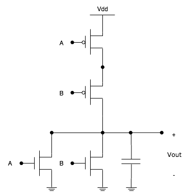
Now, let’s take a look at a pseudo-NMOS implementation of the same NOR gate:
Cell’s implementation goes one step further. The p-type transistor at the top of the circuit and the n-type transistor at the bottom are clocked on non-overlapping phases, meaning that the two clocks aren’t high/low at the same time.
The way in which the gate here works is as follows: inputs are first applied to the logic in between the clock fed transistors. The top transistor’s gate is closed allowing the logic transistors to charge up. The gate is then opened and the lower transistor’s gate is closed to drain the logic transistors to ground. The charge that remains is the output of the circuit.
What’s important about this is that since power is only consumed during two non-overlapping phases, overall power consumption is lower than static CMOS. The downside is that clock signal routing becomes much more difficult.
The other benefit is lower transistor count. In the example of the 2-input NOR gate, our static CMOS design used 4 transistors, while our pseudo-NMOS implementation used 4 transistors as well. But for a 3-input NOR gate, the static CMOS implementation requires 6 transistors, while the pseudo-NMOS implementation requires 5. The reasoning is that for a CMOS circuit, you have 1 p-type transistor for every n-type, while in a pseudo-NMOS circuit you only have two additional transistors beyond the bare minimum required to implement the logic function. For a 100-input NOR gate (unrealistic, but a good example), a static CMOS implementation would require 200 transistors, while a pseudo-NMOS implementation would only require 102.
By making more efficient use of transistors and lowering power consumption, Cell’s pseudo-NMOS logic design enables higher clock frequencies. The added cost is in the manufacturing and design stages:
- As we mentioned before, clock routing becomes increasingly difficult with pseudo-NMOS designs similar to that used in Cell. The clock trees required for Cell are probably fairly complex, but given IBM’s expertise in the field, it’s not an insurmountable problem.
- Designing pseudo-NMOS logic isn’t easy, and there are no widely available libraries from which to pull circuit designs. Once again, given IBM’s size and expertise, this isn’t much of an issue, but it does act as a barrier for entry of smaller chip manufacturers.
- Manufacturing such high speed dynamic logic circuits often requires techniques like SOI, but once again, not a problem for IBM given that they have been working on SOI for quite some time now. There’s no surprise that Cell is manufactured on a 90nm SOI process.


70 Comments
View All Comments
faboloso112 - Thursday, March 17, 2005 - link
ahh i love bedtime stories!great read...VERY informative!
ksherman - Thursday, March 17, 2005 - link
sweet article! way over my head, but there were some parts that were dropped down to my level of understanding. Leave it to anand to tell the real story. It will be interesting to see how willing some companies will be to accomidate Sony's ratical processor... bu tas long as theirs money... Do you think that it is possible to (down the road) flop a x86 chip in place of the PPE? wouldn't hat make the Cell compatible with the current processing standards?ProviaFan - Thursday, March 17, 2005 - link
Describing this as a "sit down read" type of article makes me want to print it out to put it in the magazine rack, because I don't have a laptop + 802.11g to peruse AnandTech while I'm, er... ;)xsilver - Thursday, March 17, 2005 - link
nice, definitley one of those "sit down reads".... some serious shiznit ;)cosmotic - Thursday, March 17, 2005 - link
OMG! FIRST POST LOL ROFL LMAO OMG!!! LOOK WHOS COOL!!!Fricardo - Thursday, March 17, 2005 - link
Finally! Thanks guys.Bawl - Saturday, January 25, 2014 - link
I just love this deep analysis of one of the most mist-understanding processor of the last decade.Too bad that after spending more than a half-of-billion dollars, SonyThoshibaIBM didn't release the presumably outstanding CellTwo.
Ferrx - Sunday, December 20, 2015 - link
Hi, can you help me to understand this ? I don't understand at all about these._______ _________ ______
|Decode| | Execute | | Write |
----------- ---------------- -----------
| I1 | I2 | | | | | | | |
| I3 | I4 | | I1 | I2 | | | | |
| I3 | I4 | | I1 | | | | I2 | |
| | I4 | | | | | | I1 | I3 |
| I5 | I6 | | | | I4 | | I4 | |
| | I6 | | | I5 | | | I5 | |
| | | | | I6 | | | I6 | |
_______ _________ ______
In "Decode", each row has 2 columns. What do First and Second Column mean ?
same as "Write"
And in "Execute, each row has 3 columns. What do First, Second and Third column mean ?
And how is the process ? (The current table is about "In-Order Issue with Out-of-Order Completion").
I've read it many times, in the "Instruction Level Parallelism". But I still don't have any idea about it.
Ferrx - Sunday, December 20, 2015 - link
Aww... Can't do tab-'ing' 0__0