nForce4 SLI Roundup: Painful and Rewarding
by Wesley Fink on February 28, 2005 7:00 AM EST- Posted in
- Motherboards
Gigabyte K8NXP-SLI: Features and Layout
| Specification | Gigabyte K8NXP-SLI |
| CPU Interface | Socket 939 Athlon 64 |
| Chipset | nForce4 SLI (single chip) |
| BUS Speeds | 200MHz to 400MHz (in 1MHz increments) |
| PCI/AGP Speeds | Asynchronous (Fixed) |
| PCI Speeds | 100MHz to 150MHz in 1MHz increments |
| Core Voltage | Auto, 0.80V to 1.75V in 0.025V increments |
| DRAM Voltage | Normal, +0.1V, +0.2V |
| Chipset Voltage | Normal, +0.1V, +0.2V, +0.3V |
| Hyper Transport Ratios | Auto, 1x to 5x in 1x increments |
| LDT Bus Transfer | 16/16, 16/8, 8/16, 8/8 |
| LDT Voltage | Normal, +0.1V, +0.2V, +0.3V |
| CPU Ratios | Auto, 4x to 25x in 0.5x increments |
| Cool'n'Quiet MAX FID | Auto, 8.0 to 13.0 in 0.5x increments |
| DRAM Speeds | Auto, 100, 133, 166, 200 |
| Memory Command Rate | Auto, 1T, 2T |
| Memory Slots | Four 184-pin DDR Dual-Channel Slots Unbuffered Memory to 4GB Total |
| Expansion Slots | 2 x16 PCIe Slots 2 x1 PCIe 2 PCI Slots |
| SLI Setup | Movable PCB Card |
| Onboard SATA | 4-Drive SATA 2 by nF4 PLUS 4-Drive SATA by Sil3114 |
| Onboard IDE | Two Standard nVidia ATA133/100/66 (4 drives) |
| SATA/IDE RAID | 4-Drive SATA 2 PLUS 4-Drive IDE (8 total) Can be combined in RAID 0, 1 PLUS 4-Drive SATA by Sil3114 Sil3114 Raid 0, 1, 5 |
| Onboard USB 2.0/IEEE-1394 | 10 USB 2.0 ports supported nF4 3 1394B FireWire 800 ports by TI chip |
| Onboard LAN | Dual Gigabit Ethernet PCIe by Vitesse VSC8201 PHY PCIe by Marvel 88E8053 |
| Onboard Audio | Realtek ALC850 8-Channel codec with 6 UAJ audio jacks, CD-in, front audio, and coaxial SPDIF In and Out |
| Other Features | Gigabyte Dual BIOS |
| BIOS | Award 2/01/2005 |
The shipping Gigabyte BIOS for the K8NXP-9/K8NXP-SLI family provides a wide and useful range of adjustments for many features, with the notable exception of a very limited range of memory voltage adjustments compared to other boards in the SLI roundup. As is the Gigabyte custom in recent designs, Advanced Chipset Features (and Memory Timings) can only be seen when you hot press CTRL+F1 while in the BIOS. HyperTransport adjustments are also provided in the hidden Advanced Chipset Features menu.
There are no BIOS options for adjusting or controlling SLI. This is handled in the nForce4 platform drivers and the nVidia graphics drivers.
The Gigabyte K8NXP-SLI, like the sister K8NXP-9, was designed as a top-of-the-line nForce4 motherboard. As the flagship model, it sports all the top Gigabyte features.
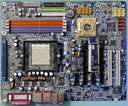
We are pleased that Gigabyte uses the nF4 on-chip Gigabit LAN by supporting it with a Vitesse (Cicada) Gigabit PHY. Gigabyte then goes one step further by including a second Gigabit LAN on the PCI Express Bus. This second LAN is also removed from the constraints of the slower PCI bus as it resides on the much faster PCIe bus.
Audio is AC '97 2.3, supported by the popular 8-channel Realtek ALC850. The K8NXP-SLI9 includes a wide range of audio I/O provided to make the most of the 850 chip. This includes 6 programmable audio mini-jacks and coax SPDIF in and out - all on the rear panel.
A pioneering feature for Gigabyte has been their support of high-speed 1394B Firewire on their boards. This continues with the K8NXP-SLI with 2 ports capable of 800MB/s or Firewire 800. This is double the speed of 1394A for those looking for fast Firewire access.
From a feature, board layout, and BIOS options point of view, the K8NXP-SLI can be considered the twin of the K8NXP-9. The only real change is the replacement of one PCI slot with a second PCIe video slot. All the good things about the features and layout of the K8NXP-9 are still here in the K8NXP-SLI.
DFI LANParty nF4 SLI-DR: Overclocking and Stress Testing
Gigabyte K8NXP-SLI: Overclocking and Stress Testing


108 Comments
View All Comments
fitten - Tuesday, March 1, 2005 - link
quote:I still do not understand why this argument is so popular. Why is the general assumption that purchasers of SLI capable boards will immediately want to jump into a dual-card config? The idea is flexibility. Sure, 2 6800's are expensive now, but they will inevitably get cheaper.Well, if history serves as a measure... by the time that 2nd board becomes cheap enough to justify its cost, there will be a new board out (say, the nVidia 7800) that will be as fast, or faster than, the SLI combo.
I used to buy motherboards with two sockets for this very reason (flexibility to upgrade to two CPUs later) until about twice doing this I learned that by the time I was ready for that 2nd CPU, there was one out that was faster than both put together.
Computers change too fast. If you perpetually buy on the bleeding edge, you cannot plan any upgrades past ~6 months and definitely not past 12 months. By that time, you'll throw away what you have and get the NextBestThing(tm). Buying SLI is bleeding edge. Saying that you'll buy the upgrade card in a year is just a rationalization to buy the bleeding edge now.
Aquila76 - Tuesday, March 1, 2005 - link
Yeah, that's right. Some apps run slower with SLI because nVidia hasn't SLI optimized the driver for that app (so it can then only utilize one card) and the SLI setup uses some overhead, resulting in slower results. Any new game/benchmark will use SLI just fine. The results in Half-Life and Doom 3 as well as if you add the config for stuff like NFS:U2 and whatever are well above one card though.Sunbird - Tuesday, March 1, 2005 - link
Is my brain screwed up or are the 3Dmark03 single scores higher than the SLI scores???chup - Tuesday, March 1, 2005 - link
too bad, i thought the MSI was the one to get after nforce2.sphinx - Tuesday, March 1, 2005 - link
From this review, I have come to the conclusion that ASUS is slipping. I have always been a supporter of ASUS but, I think this review shows how much ASUS is all about the money and not making quality products. Right now I am waiting for manufacturers to get the VIA chipset working properly. I haven't seen many news or reviews on VIA's new chipset. One other thing. Who in their right mind would spend close to $250 on nVidia's NF4 if there is really no significant performance jump from the NF3.bigbusa - Tuesday, March 1, 2005 - link
You mentioned the asus manual says use a 500+W PS. if you read the Asus users guid the sli 6800 ultra system also has all pci slots used, all memory dims full, 2 optical drives, and anassortment of other stuff. and they recommend a 500+W, but a 350W PS for a dual 6600GT. See below.500+W ps for 55FX, 2x6800 ultra, 4ddr dims, 4 HD's, 2 optical, 1 pcie 1x card, 3 pci card, 1 1394, 6 usp devices. (shit thats alot of gear)
350W for a 3400(64bit 939), dual 6600GT, 2 DDRdims, 2 hd's, 1 optical drive, no pcie 1x, 1 pci card, no 1394, and 3 usb devices.
SO the article is misleading a bit.
The review also did not cover any quad displays and problems one may encounter when setting this up.
Reflex - Tuesday, March 1, 2005 - link
#70 - None of these boards support ECC. The reason for that is that such support would be implemented by the memory controller, not the motherboard manufacturer. In this particuliar case the memory controller is integrated into the CPU. AMD has a line of CPU's that have ECC support, they are called the Opteron and are designed for workstations and servers.In the home user market ECC does not significantly impact stability but it does harm performance by a small amount which is why the feature is not generally available on consumer solutions.
1955mm - Tuesday, March 1, 2005 - link
All in all I think that this is the best review of Socket 939 SLI boards that I have seen. I particularly liked the attention paid to storage and I/O capabilities. My one criticism is that although comments were made regarding stability, and a link was made between overclocking and stability, there was no discussion of ECC support. If system reliability is discussed, ECC should not be ignored. As far as I can tell, the only board supporting ECC is the ASUS board. Over the years I have found it difficult to get accurate information on ECC support, having been given misleading information on occasion by both MSI and ASUS.Aquila76 - Tuesday, March 1, 2005 - link
D'oh, *SoundSTORM Savior*That's it, I'm off to bed. It's quarter of 1:00AM and I have work tomorrow. Uh, today.
Aquila76 - Tuesday, March 1, 2005 - link
To everyone hoping the MSI upsamples analog 5.1 to Dolby Digital - I don't think so. Like any Creative card, it can either downmix DD-EX/DTS-ES 7.1 streams to 4/5.1 speakers (which is what page 5-11 of the manual is actually talking about doing), decode DD/DTS on-card to 5/6/7.1 speakers (via analog or 'Digital Out', Creative's proprietary digital link for their speaker sets), or can just pass the Dolby Digital/DTS 5/6/7.1 signal (now via the SPDIF coax/optical cable) to any outboard decoder.I say this because I have the same exact chip on a stand-alone card, and it does not upsample analog sound to Dolby Digital, like SoundStorm did. 'Digital Out' simply let's you use a proprietary Creative Digital DIN connector to connect one cable from the soundcard to the Creative speaker amp (like on a DTT3500 that I use).
I also find it highly unlikely that Creative would license a DD Live capable chip to only one manufacturer when they have yet to produce one of their own cards with this feature.
*Keeps waiting for a SoundStrom Saviour*