Intel's Architecture Day 2018: The Future of Core, Intel GPUs, 10nm, and Hybrid x86
by Dr. Ian Cutress on December 12, 2018 9:00 AM EST- Posted in
- CPUs
- Memory
- Intel
- GPUs
- DRAM
- Architecture
- Microarchitecture
- Xe
Demonstrating Sunny Cove and Gen11 Graphics
As part of the Architecture Event, Intel ran a number of demos on a chip that was supposedly based on the new Sunny Cove cores and Gen11 graphics.
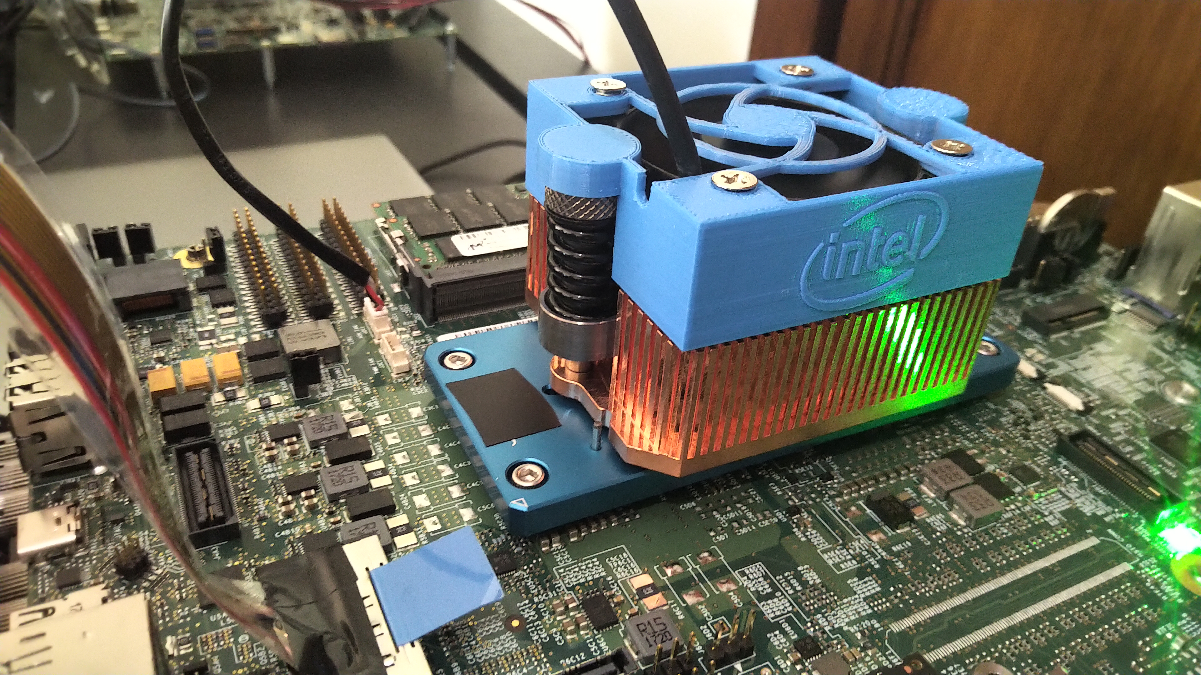
These were development systems with these funky looking heatsinks and loud fans to ensure there was no thermal throttling. One thing worth noticing is that black bit of tape on the heatsink here, which wasn’t present on one of the other demo units.
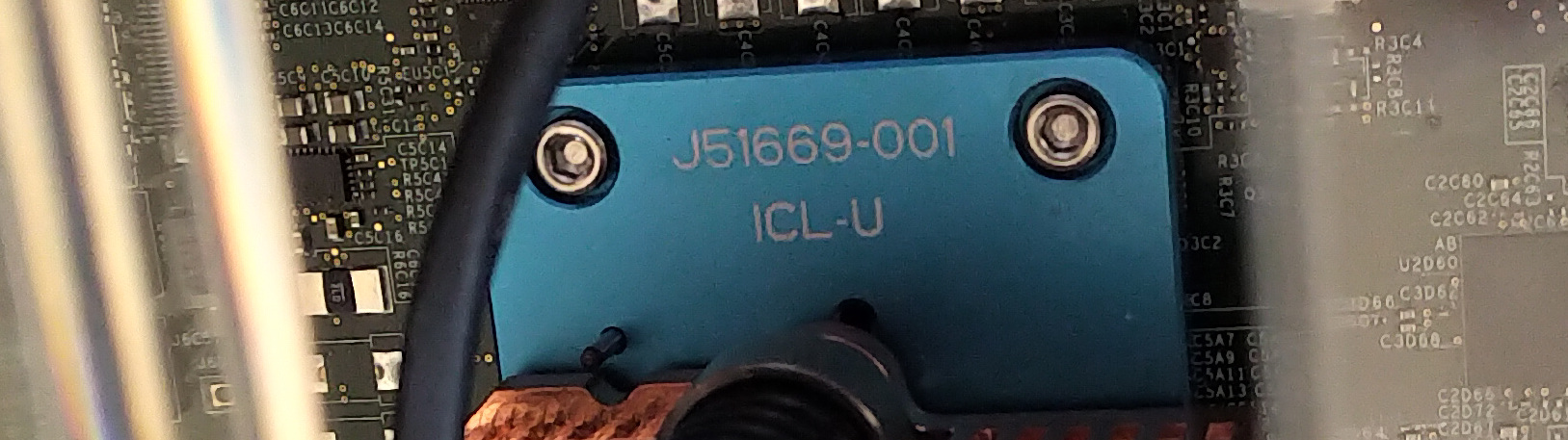
Hello Ice Lake-U. Being a U-series heatsink, this means that the Core is likely designed for a 15W scenario.
Perhaps it’s no surprise that Intel wasn’t giving anything away in terms of the exact core count on display, speeds, feeds, and power. The demos that were present involved 7-Zip and gaming.
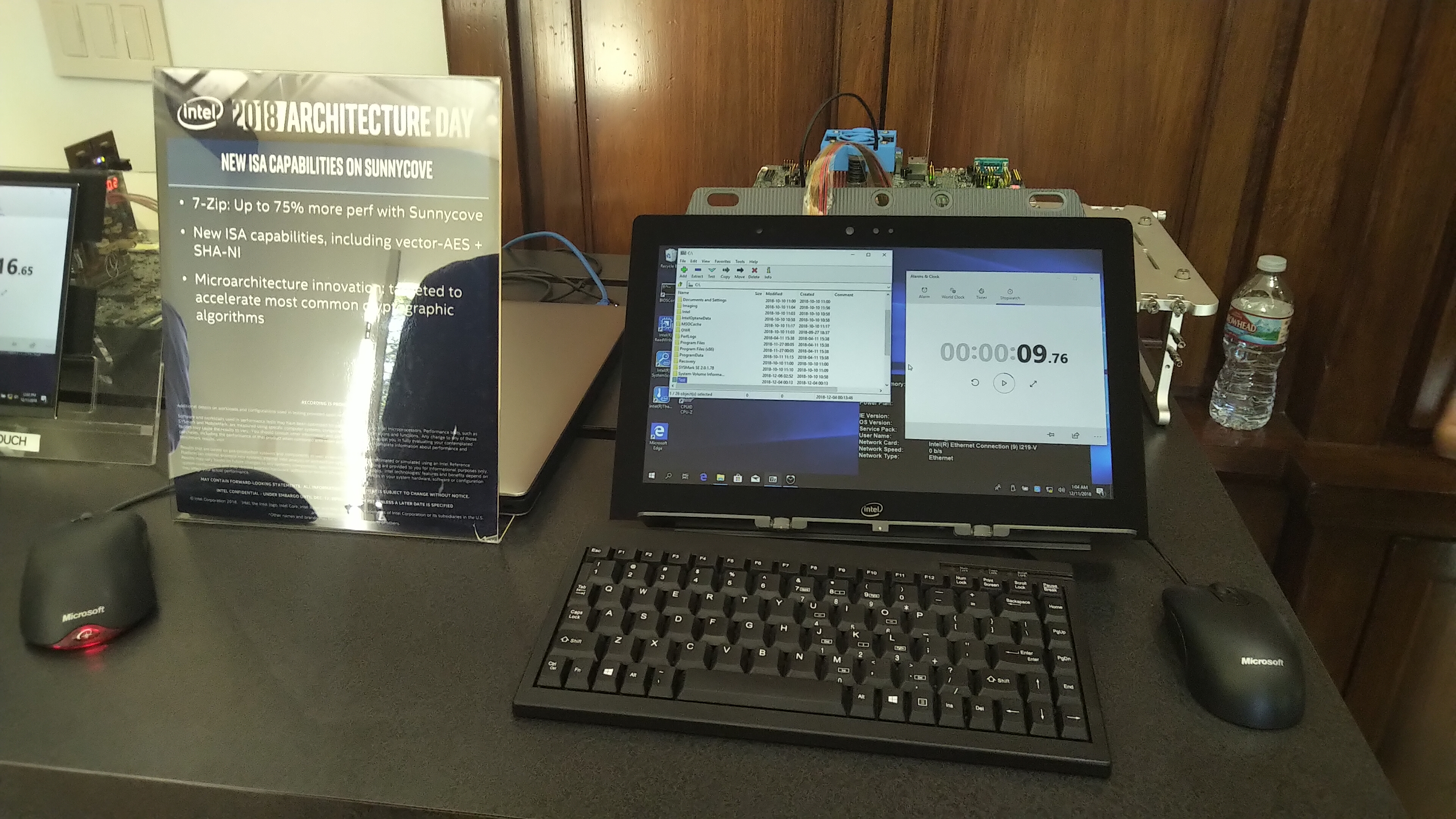
The 7-Zip demo was relatively straight forward, showing how the new instructions such as Vector-AES and SHA-NI in Sunny Cove can give the processor a 75% boost in performance over an equivalent Skylake based platform at iso-frequency. This falls under the ‘specialist’ improvements to the core rather than the general purpose improvements.
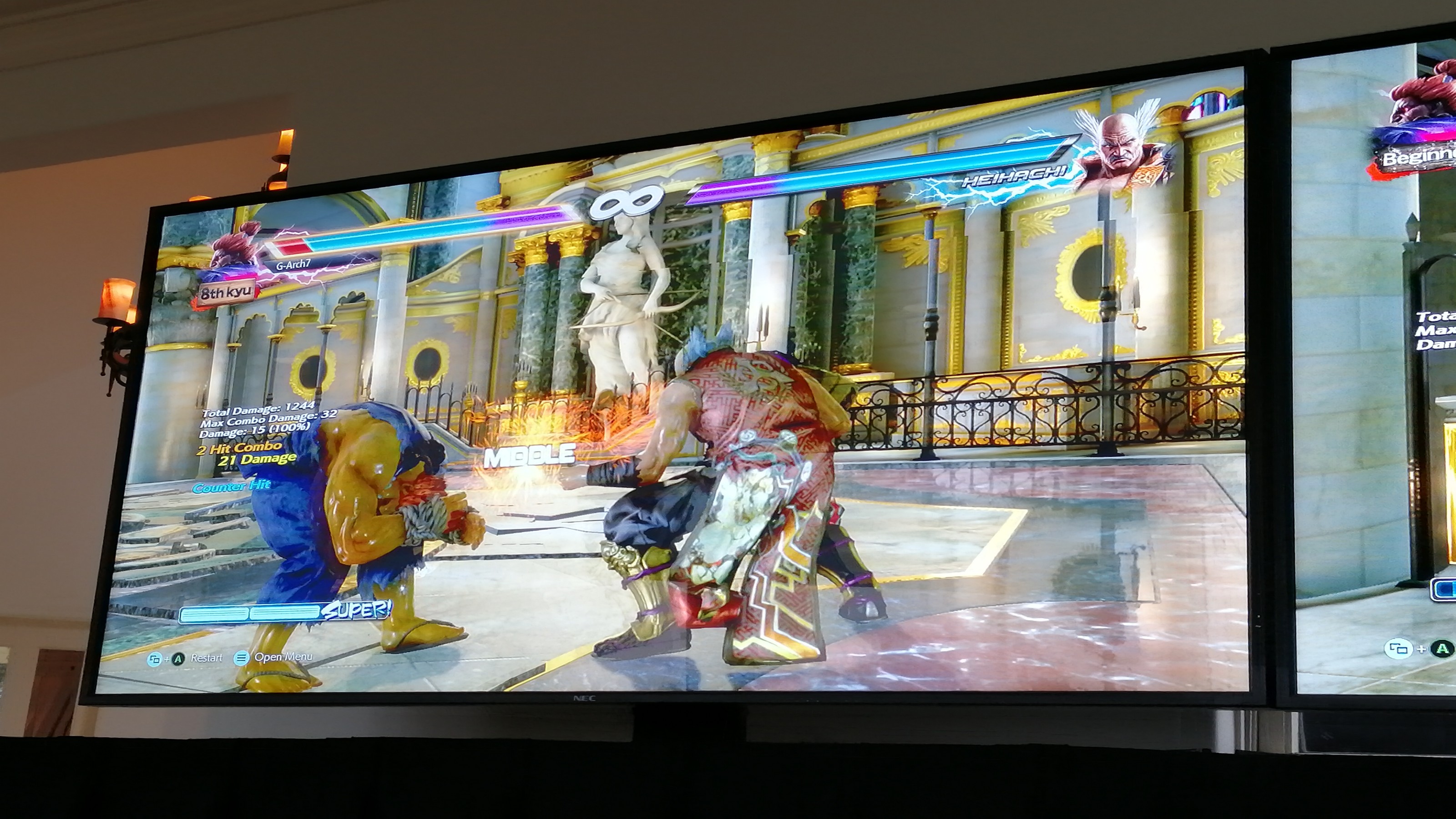
The other demo was Tekken 7, being run on a Sunny Cove + Gen11 machine and compared to a Skylake + Gen9 implementation. It looked a good deal smoother that’s for sure, however it was clear that it had some way to go to be fully out of the 30 FPS minimums.


148 Comments
View All Comments
johannesburgel - Wednesday, December 12, 2018 - link
"We have a new method inside the company to decouple IP from the process technology. You must remember that customers buy the product, not a transistor family. It’s the same transformation AMD had to go through to change the design methodology when they were struggling."...doesn't that basically mean they're going fabless, or are at least going to develop a design for multiple processes so they can also use other fabs as well? Not that I'm disagreeing with that! If I was Intel I would have started doing so years ago, when everybody else was starting to do it.
anonomouse - Wednesday, December 12, 2018 - link
I think this just means fewer hand placed/routed custom logic blocks, and more synthesis/APR. If you look at most other dies these days, you see a sea of gates. When you look at intel dies, in the cpu cores you see very tight, regular logic blocks. Every mention of "abstraction" in the Q&A screamed synthesis/APR. This may make it possible for them to port to other foundries if they wanted to, but I doubt they would.An interesting question is whether this has any implications to power/timing/area optimization vs. the current approach, as a lot of their ability to push very high clocks might come from how much more custom logic design goes into their implementation.
kapg - Wednesday, December 12, 2018 - link
I guess in the image Intel 'CPU Core Roadmap' for Atom the name 'Next' Month is a typo from IntelAlexvrb - Wednesday, December 12, 2018 - link
"quad-channel memory controller (4x16-bit)"Well, we know the GPU won't be competitive with upcoming ARM designs, then. Otherwise, very neat mobile class chip design.
Arbie - Wednesday, December 12, 2018 - link
"Golden Cove ... is firmly in that 2021 segment ... we’re likely to see it on 10nm and or 7nm."Likely? If it isn't one of those two it will be big news indeed.
HStewart - Thursday, December 13, 2018 - link
10nm is already stated for Sunny Cove in 2019, so it likely 7nm - but keep in mind the process (nm) is decouple for process - so it could be 10nm or 7nmajc9988 - Wednesday, December 12, 2018 - link
Ian, the active interposer isn't new, and I am wanting o know more exactly what has been moved to the active interposer. AMD's whitepapers on the topic, using routers, etc., on an active interposer, was published in 2014 and a follow up on 2015. In late 2017, AMD published a white paper dealing with the costs of doing so, where producing an active interposer on smaller than 40nm resulted in costs being the same as producing a monolithic die. AdoredTV did two videos on this topic months ago, as a matter of fact. So, unless they are sticking some of the features that AMD put on the I/O die onto the active interposer, this is doing what AMD plans to do but chose not to on the basis of cost. Check out these papers and videos:http://www.eecg.toronto.edu/~enright/micro14-inter... http://www.eecg.toronto.edu/~enright/Kannan_MICRO4... https://youtu.be/G3kGSbWFig4 https://seal.ece.ucsb.edu/sites/seal.ece.ucsb.edu/... https://www.youtube.com/watch?v=d3RVwLa3EmM&t=...
Intel seems to now be using ideas from everywhere else in the industry, while also using 22nm fabs that would have been slated for decommission if not for the 10nm fiasco that is their process, which they had to push certain chipsets to due to the 14nm shortage, meaning they need to keep the fab time full to justify them keeping the lights on and a 22nm active interposer fits the bill. The article practically writes itself.
iwod - Thursday, December 13, 2018 - link
No news on opening up TB3? Which they promised to do in 2018.The Hybrid, I wish it had two HP Core. but 7W is actually the same TDP for MacBook Air Retina.
The_Assimilator - Thursday, December 13, 2018 - link
Thunderbolt is dead in mainstream PCs at this point, because there's no use-case in which it outperforms USB by enough to justify its cost (both of implementation and in the peripherals that people actually want to use). It's become another almost-Mac-exclusive like Firewire, and will share the same fate.gamerk2 - Thursday, December 13, 2018 - link
Yep, this pretty much the same thing that happened to Firewire. Thunderbolt never had a reason to exist; USB3 handles pretty much every TB3 use-case.