Gigabyte 7NNXP (nForce2 Ultra 400): Gigabyte Goes nForce
by Evan Lieb on July 5, 2003 10:53 PM EST- Posted in
- Motherboards
Gigabyte 7NNXP: BIOS and Overclocking
Gigabyte continues to utilize the Award BIOS on 100% of their desktop motherboards with the 7NNXP.
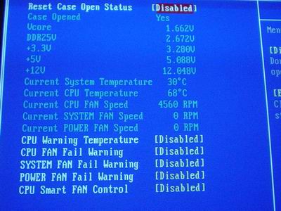
The 7NNXP PC Health section includes such readings as System and CPU temperatures, CPU, System, and Power fan speeds, Vcore, VDIMM, and PSU readings (all rails). Gigabyte adds in other options, such as a “CPU Smart Fan Control” option that regulates the speed of your CPU HSF depending on the task at hand. Unfortunately, this option cannot be adjusted or tweaked in any way; you can only disable or enable CPU Smart Fan Control. Other features that you can use in the PC Health section are CPU/System/Power Fan Fail Warning options, which can be enabled or disabled, and a CPU Warning Temperature option that, when enabled, will shut down your system (90C is the maximum value you can set this option).
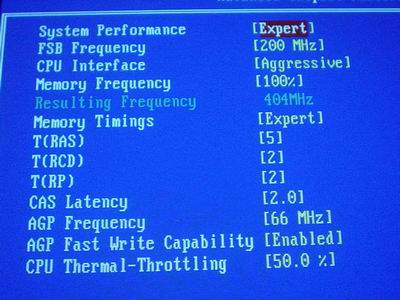
Gigabyte continues the tradition of using the CTRL + F1 method of revealing memory-related tweaking options in the BIOS. However, the 7NNXP BIOS does not hide the Advanced Chipset Features section like in previous Gigabyte motherboards. This time, holding the CTRL key and pressing F1 simply reveals more tweaking options within the Advanced Chipset Features section (make sure to press CTRL + F1 outside of the Advanced Chipset Features section, not inside). Anyway, this section contains the usual collection of memory timing options, such as CAS Latency, RAS to CAS Delay, RAS Precharge, and Precharge Delay. There are also other very important performance-related options, such as FSB frequency, AGP frequency, memory frequency, AGP fast write option and, finally, the CPU interface option (Aggressive or Optimal available). This is a very well organized and structured Advanced Chipset Features section. However, we would prefer it if Gigabyte would leave out the CTRL + F1 setting in future BIOSes, unless of couse Gigabyte’s research has proven that it causes fewer problems with end users who are novices at setting up a BIOS.
As mentioned, there are FSB frequency adjustments available in the Advanced Chipset Features section. The 7NNXP FSB ceiling is 300MHz FSB, which is more than enough for the most adventurous overclockers out there. You will never reach anywhere near this frequency reliably, so don’t worry about maxing out your CPU’s FSB anytime in the future, especially since AMD will not be using anything higher than a 400MHz FSB when the Athlon eventually dies.
Gigabyte offers decent VDIMM control within the 7NNXP BIOS. VDIMM is available up to 2.8V in 0.1V increments. This should be plenty for the vast majority of users out there. However, for those users who aren’t pleased with 2.8V, you may find it comforting to know that the 7NNXP naturally overvolts by 0.07V; thus, 2.87V is the maximum attainable memory voltage the 7NNXP can reach.
The Vcore options available in the 7NNXP BIOS are adequate, though not all that great. Vcore is available as high as 1.850V in 0.0250V increments. The increments in which Vcore can be tuned is more disappointing than the somewhat low Vcore ceiling. We would have preferred 0.0125V adjustments instead, as finer adjustments are never a bad thing and can be easily implemented. Still, 0.0250V should suffice for most users. The 1.850V ceiling should also be more than enough for most overclockers, though there will undoubtedly be adventurous overclockers that will want to push further than 1.850V. In those cases the 7NNXP does not fit the bill.
According to Gigabyte, the AGP and PCI buses are locked at their default frequencies (66MHz/33MHz) regardless of the FSB frequency. The AGP lock is evident from looking at the AGP frequency options in the Advanced Chipset Features section. On the other hand, the PCI lock is hidden and cannot be independently adjusted like the AGP bus. Nevertheless, the 7NNXP still has an AGP/PCI lock and that’s all that matters.
The VAGP adjustments available in the 7NNXP BIOS are just fine. VAGP is adjustable in 0.1V increments up to 1.8V, and should suit just about anyone looking to increase their VAGP.
One final feature that adds a nice touch to the 7NNXP is chipset voltage adjustments. The 7NNXP BIOS allows chipset voltage adjustments of 5%, 7.5%, and 10%. Thankfully the nForce2 Ultra 400 North Bridge onboard the 7NNXP is equipped with an active North Bridge heatsink, otherwise we would have suggested the addition of active cooling.


29 Comments
View All Comments
Anonymous User - Tuesday, July 8, 2003 - link
Yes, uhm, can we go back to GIF? I hate Flash. Look, I'm on dialup, and I'm lagged a LOT by big downloads, but I still prefer GIFs to Flash (which seems to load a tad faster). My friends all agree, and most of them are dialuppers too. Please, at least put up a poll or something so you can see how we all really feel about this stupid Flash stuff.NovaPolice - Monday, July 7, 2003 - link
It looked very good on paper but it hated every brand of ddr I had on hand. I went through a couple gigs of sticks before deciding to send it back.Anonymous User - Monday, July 7, 2003 - link
I have tested both this board, and the MSI K7N2Delta. The MSI board was FAR MORE stable, and a bit (7%) faster. I wonder why in this test the Gigabyte board is compared with an EPOX via board: Just to let it outperform, which is otherwise not possible?Anonymous User - Monday, July 7, 2003 - link
They say that CPU voltage is adjustable only up to 1.85v and that chipset voltage is adjustable by 5, 7.5 or 10%. I believe this to be wrong however. What the reviewer believes to be chipset voltage is actually CPU voltage also!! Check out the review over at Digital Daily and they show how voltage up to 2.035v is possible using a combination of these 2 seperate CPU voltage controls! Quite a large difference and large overlook by the reviewer.WooDaddy - Monday, July 7, 2003 - link
Evan, are you or anyone at Anandtech going to discuss the differences between the Ultra 400 and the standard nForce 2 chipsets? Maybe a general review with reference boards? Is there a big performance difference or limiting factor for future upgrades?Anonymous User - Monday, July 7, 2003 - link
The review does not include information on the presence of Heat Sink Mounting Holes. Suggestion, add info on mounting holes or lack of to all motherboard reveiws.Anonymous User - Monday, July 7, 2003 - link
It appears that the performance test results in the Gigabyte 7NNXP review are presented in Macromedia Flash Player 6.This is unfortunate, since I am among the many web users who dislike the Flash format, and resent the numerous pop-up "ads" requesting that version 6 be installed.
I regret that I will be unable to view these results, to find out what additional complexities required them to be displayed in Flash, rather than a standard, multi-platform/browser form such as GIFs. And I hope that this is not an indication that future results will be Flash-formatted, since I am a frequent AnandTech reader and will miss whatever informative content is Flashed.
Thanks.
Anonymous User - Sunday, July 6, 2003 - link
The Anandtech review claims Gigabyte replied in 33 hours..I Wonder who in Gigabyte Should I contact ,Or what e-mail address i should mail to,
To get a Reply in ANY time frame.
CrystalBay - Sunday, July 6, 2003 - link
Nice evaluation...However perhaps the six phase power DMS prolongs the overall life of these boards, rather than inherently more stable overclocking...Replacing a board thirteen months, two or three years down the line (If lucky) is common place...I like to see more board makers produce the bare bones 400's like Solteks NV400-64L...Why because these boards can be thrown away once a year or so...