The Intel Core i3-7350K (60W) Review: Almost a Core i7-2600K
by Ian Cutress on February 3, 2017 8:00 AM ESTPower Consumption
As with all the major processor launches in the past few years, performance is nothing without a good efficiency to go with it. Doing more work for less power is a design mantra across all semiconductor firms, and teaching silicon designers to build for power has been a tough job (they all want performance first, naturally). Of course there might be other tradeoffs, such as design complexity or die area, but no-one ever said designing a CPU through to silicon was easy. Most semiconductor companies that ship processors do so with a Thermal Design Power, which has caused some arguments recently based presentations broadcast about upcoming hardware.
Yes, technically the TDP rating is not the power draw. It’s a number given by the manufacturer to the OEM/system designer to ensure that the appropriate thermal cooling mechanism is employed: if you have a 65W TDP piece of silicon, the thermal solution must support at least 65W without going into heat soak. Both Intel and AMD also have different ways of rating TDP, either as a function of peak output running all the instructions at once, or as an indication of a ‘real-world peak’ rather than a power virus. This is a contentious issue, especially when I’m going to say that while TDP isn’t power, it’s still a pretty good metric of what you should expect to see in terms of power draw in prosumer style scenarios.
So for our power analysis, we do the following: in a system using one reasonable sized memory stick per channel at JEDEC specifications, a good cooler with a single fan, and a GTX 770 installed, we look at the long idle in-Windows power draw, and a mixed AVX power draw given by OCCT (a tool used for stability testing). The difference between the two, with a good power supply that is nice and efficient in the intended range (85%+ from 50W and up), we get a good qualitative comparison between processors. I say qualitative as these numbers aren’t absolute, as these are at-wall VA numbers based on power you are charged for, rather than consumption. I am working with our PSU reviewer, E.Fylladikatis, in order to find the best way to do the latter, especially when working at scale.
Nonetheless, here are our recent results for Kaby Lake at stock frequencies:
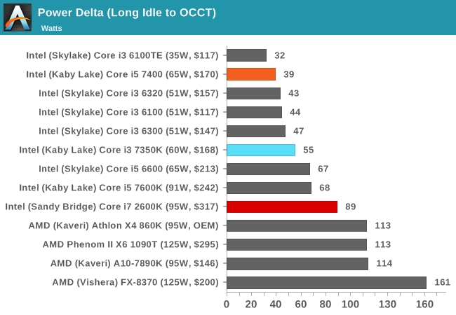
The Core i3-7350K, by virtue of its higher frequency, seems to require a good voltage to get up to speed. This is more than enough to go above and beyond the Core i5, which despite having more cores, is in the nicer part (efficiency wise) in the voltage/frequency curve. As is perhaps to be expected, the Core i7-2600K uses more power, having four cores with hyperthreading and a much higher TDP.
Overclocking
At this point I’ll assume that as an AnandTech reader, you are au fait with the core concepts of overclocking, the reason why people do it, and potentially how to do it yourself. The core enthusiast community always loves something for nothing, so Intel has put its high-end SKUs up as unlocked for people to play with. As a result, we still see a lot of users running a Sandy Bridge i7-2600K heavily overclocked for a daily system, as the performance they get from it is still highly competitive.
There’s also a new feature worth mentioning before we get into the meat: AVX Offset. We go into this more in our bigger overclocking piece, but the crux is that AVX instructions are power hungry and hurt stability when overclocked. The new Kaby Lake processors come with BIOS options to implement an offset for these instructions in the form of a negative multiplier. As a result, a user can stick on a high main overclock with a reduced AVX frequency for when the odd instruction comes along that would have previously caused the system to crash.
For our testing, we overclocking all cores under all conditions:
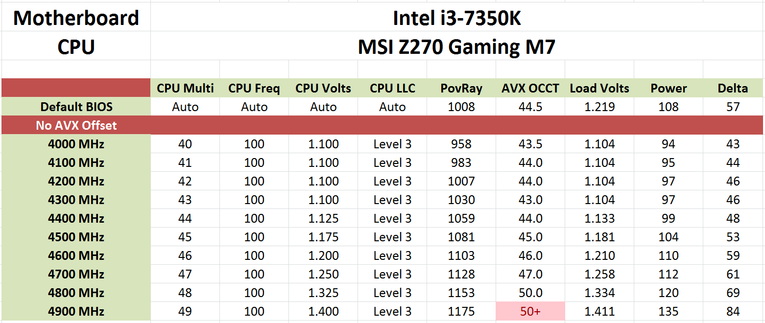
The overclocking experience with the Core i3-7350K matched that from our other overclockable processors - around 4.8-5.0 GHz. The stock voltage was particularly high, given that we saw 1.100 volts being fine at 4.2 GHz. But at the higher frequencies, depending on the quality of the CPU, it becomes a lot tougher maintain a stable system. With the Core i3, temperature wasn't really a feature here with our cooler, and even hitting 4.8 GHz was not much of a strain on the power consumption either - only +12W over stock. The critical thing here is voltage and stability, and it would seem that these chips would rather hit the voltage limit first (and our 1.4 V limit is really a bit much for a 24/7 daily system anyway).
A quick browse online shows a wide array of Core i3-7350K results, from 4.7 GHz to 5.1 GHz. Kaby Lake, much like previous generations, is all about the luck of the draw - if you want to push it to the absolute limit.


186 Comments
View All Comments
JordanV - Tuesday, February 14, 2017 - link
I think the sales argument for the big Intel chips as video encoders has been for x264 where the faster NVENC, VCE, and QuickSync technologies offer lower quality at a given bitrate for higher quality x264 settings. For most people, the hardware encoders are enough but for many others, the quality is not sufficient.The quality difference between hardware and software HEVC is smaller with higher quality software h265 encodes beating the quality of your Pascal x265 encodes but with a big performance penalty. It's not worth it for most people, but if you have limited bitrate/storage and want the best quality, it might be.
HerrKaLeun - Friday, February 3, 2017 - link
Thanks for the great review, Ian.Considering one needs an expensive Z-board to OC, for most people buying an i5 makes more sense.
I don't understand why so many people complain about Intel allegedly not making enough progress. Now you get a dual-core that comes close (or even exceeds in single threaded benches) to the former flagship quadcore. If you want to have a CPU that vastly exceeds the "old" quadcore, Intel also has newer quadcores. It is not like the i3 is the end of the lineup.... For the $317 that the 2600k used to cost you can get a KabyLake non-K i7, which sure vastly exceeds in performance (and much lower TDP). I assume someone who could afford an over $300 CPU 6 years ago can afford $300 now and upgrading to an i3 may not be what that person would do anyway. the trend goes to more cores.... most people here complain about Intel not offering mainstream hexa and octa cores... not sure why the same people allegedly are so eager to get dual-cores.
zodiacfml - Friday, February 3, 2017 - link
Dual core is too weak for me. Web browsing can use more cores.Hulk - Friday, February 3, 2017 - link
Sorry to be dense.What does 2+2, 4+2, 4+3/e mean?
babysam - Saturday, February 4, 2017 - link
The first number refers to the number of CPU cores. Te second number refers to the IGP configuration (the number of shaders, which may be a little bit different across generations, e.g. Haswell GT3 has 40 shaders, while Broadwell/Skylake GT3 have 48 shaders).The extra e means there is an extra eDRAM cache (Crystalwell) on the CPU package.
Hulk - Saturday, February 4, 2017 - link
Thanks.AndrewJacksonZA - Saturday, February 4, 2017 - link
Thank you babysam.babysam - Saturday, February 4, 2017 - link
Thank you for you article (especially when many of us are waiting on the information of new CPU of both AMD and Intel). It is always good to have something to play (overclocked) with, but this is a little bit expensive.When I read the analysis of the first page, I see the lack of information on the CPU die size and transistor count disclosed by Intel recently. Also, I feel strange that the effect of the change of the 32nm to 22nm (from Haswell to Broadwell) have such a large difference on the 2C+GT2(which Intel claims there is a 37% reduction of the die, which can be seen in the table) and the 4C+GT3(which the difference are much smaller) CPU die. I feel even stranger when I see the Skylake 4C+GT3e die is a bit smaller than the Broadwell 4c+GT3e die. So I am quite curious on the sources of the die estimate.
P.S. I found the origin of the 234mm^2 of the Skylake die size estimate.
https://techreport.com/forums/viewtopic.php?t=1177...
which based on the images of the following
http://www.anandtech.com/show/10281/intel-adds-cry...
It seems that the die described is the Skylake-H(which is a 4C+GT4e configuration). This makes the 241.5mm^2 estimate of the Broadwell 4C+GT3e a little bit unrealistic (Skylake GT4e have 72 shaders, while Broadwell GT3e have 48 only)
babysam - Saturday, February 4, 2017 - link
Just find the die size of the Broadwell-H (4C+3e) in this documenthttp://www.intel.com/content/www/us/en/embedded/pr...
According to the document, the die size of Broadwell-H (4C+GT3e) should be 13.7mmx12.3mm = 168.51mm^2
(Many thanks for the hints: https://forums.anandtech.com/threads/broadwell-cor... , which the got the answer two years ago.)
WoodyBL - Saturday, February 4, 2017 - link
Am I the only one noticing that the i5-4690 was beating the i5-7600k in a lot of benchmarks? I'm having a hard time processing how that was even possible...