AMD Zen Microarchitecture: Dual Schedulers, Micro-Op Cache and Memory Hierarchy Revealed
by Ian Cutress on August 18, 2016 9:00 AM ESTDeciphering the New Cache Hierarchy
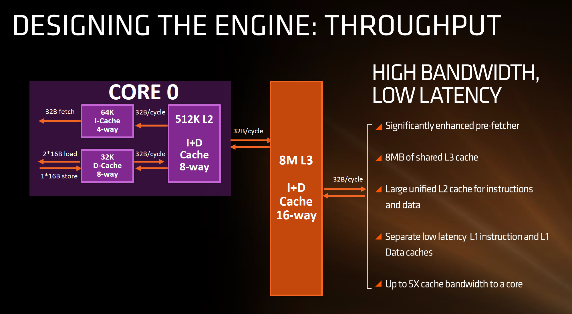
The cache hierarchy is a significant deviation from recent previous AMD designs, and most likely to its advantage. The L1 data cache is both double in size and increased in associativity compared to Bulldozer, as well as being write-back rather than write-through. It also uses an asymmetric load/store implementation, identifying that loads happen more often than stores in the critical paths of most work flows. The instruction cache is no longer shared between two cores as well as doubling in associativity, which should decrease the proportion of cache misses. AMD states that both the L1-D and L1-I are low latency, with details to come.
The L2 cache sits at half a megabyte per core with 8-way associativity, which is double that of Intel’s Skylake which has 256 KB/core and is only 4-way. On the other hand, Intel’s L3/LLC on their high-end Skylake SKUs is at 2 MB/core or 8 MB/CPU, whereas Zen will feature 1 MB/core and both are at 16-way associativity.
Edit 7:18am: Actually, the slide above is being slightly evasive in its description. It doesn't say how many cores the L3 cache is stretched over, or if there is a common LLC between all cores in the chip. However, we have recieved information from a source (which can't be confirmed via public AMD documents) that states that Zen will feature two sets of 8MB L3 cache between two groups of four cores each, giving 16 MB of L3 total. This would means 2 MB/core, but it also implies that there is no last-level unified cache in silicon across all cores, which Intel has. The reasons behind something like this is typically to do with modularity, and being able to scale a core design from low core counts to high core counts. But it would still leave a Zen core with the same L3 cache per core as Intel.
| Cache Levels | ||||
| Bulldozer FX-8150 |
Zen | Broadwell-E i7-6950X |
Skylake i7-6700K |
|
| L1 Instruction | 64 KB 2-way per module |
64 KB 4-way | 32 KB 8-way | 32 KB 8-way |
| L1 Data | 16 KB 4-way Write Through |
32 KB 8-way Write Back |
32 KB 8-way Write-Back |
32 KB 8-way Write-Back |
| L2 | 2 MB 16-way per module |
512 KB 8-way | 256 KB 8-way | 256 KB 4-way |
| L3 | 1 MB/core 64-way |
1 or 2 MB/core ? 16-way |
2.5 MB/core 16/20-way |
2 MB/core 16-way |
What this means, between the L2 and the L3, is that AMD is putting more lower level cache nearer the core than Intel, and as it is low level it becomes separate to each core which can potentially improve single thread performance. The downside of bigger and lower (but separate) caches is how each of the cores will perform snoop in each other’s large caches to ensure clean data is being passed around and that old data in L3 is not out-of-date. AMD’s big headline number overall is that Zen will offer up to 5x cache bandwidth to a core over previous designs.


216 Comments
View All Comments
Ro_Ja - Thursday, August 18, 2016 - link
I just want Zen and hope people who are waiting for it won't be disappointed.MrSpadge - Thursday, August 18, 2016 - link
"Unlike Bulldozer, where having a shared FP unit between two threads was an issue for floating point performance, Zen’s design is more akin to Intel’s in that each thread will appear as an independent core and there is not that resource limitation that BD had. With sufficient resources, SMT will allow the core instructions per clock to improve"Ian, this section makes no sense! The reason Bulldozer and kids were slow was not the module design, but simply the cores being too weak. What helps Zen is not SMT but rather the fatter cores and the power optimization. If Zen had only 2 FP execution units, the maximum FP throughput per clock would be the same as for Bulldozer, independent of whether 1 or 2 threads run on a core / module. Or similarly if a Bulldozer module would have gotten 4 FPUs.
Nagorak - Thursday, August 18, 2016 - link
As I understand it the issue was that for many purposes Bulldozer cores were really only dual core, not four true cores.TheinsanegamerN - Friday, August 19, 2016 - link
bulldozer had one FPU (a weaksauce FPU at that) for two cores, zen will have one FPU per core, the way intel does it.jjj - Thursday, August 18, 2016 - link
You list Broadwell-E L3$ at 1.5MB per core but they got 2.5.AMD with less cache and likely 2 mem chans might get away with substantially lower power and smaller die as well as lower BOM for system builders and only a minor perf penalty in consumer.
SunnyNW - Thursday, August 18, 2016 - link
Seems they wanted some press since this week and since they have a Zen presentation at Hot Chips next week anyway the timing doesnt hurt.SunnyNW - Thursday, August 18, 2016 - link
Wow that got sent ALL wrong lol....With them presenting at Hot Chips next week anyway grabbing some press this week doesnt hurt.
extide - Thursday, August 18, 2016 - link
OMG, SO excited for this. Gotta say that the FinFet GPU's and Zen are some of the most anticipated releases in a long time! I remember when I used to get excited about Intel releasing new arch's but these days that's so boring!SunnyNW - Thursday, August 18, 2016 - link
"We’ve got another couple of pieces detailing some of the AMD internal/live benchmark numbers during the presentation, as well as the dual socket server platform, the 32-core Naples server CPU, and what we saw at the event in terms of motherboard design. "Please hurry up and publish these benchmark numbers!! :)
SunnyNW - Thursday, August 18, 2016 - link
NICE!!https://www.youtube.com/watch?v=oQS8s7TOXsE