AMD Zen Microarchitecture: Dual Schedulers, Micro-Op Cache and Memory Hierarchy Revealed
by Ian Cutress on August 18, 2016 9:00 AM EST
In their own side event this week, AMD invited select members of the press and analysts to come and discuss the next layer of Zen details. In this piece, we’re discussing the microarchitecture announcements that were made, as well as a look to see how this compares to previous generations of AMD core designs.
AMD Zen
Prediction, Decode, Queues and Execution
First up, let’s dive right into the block diagram as shown:
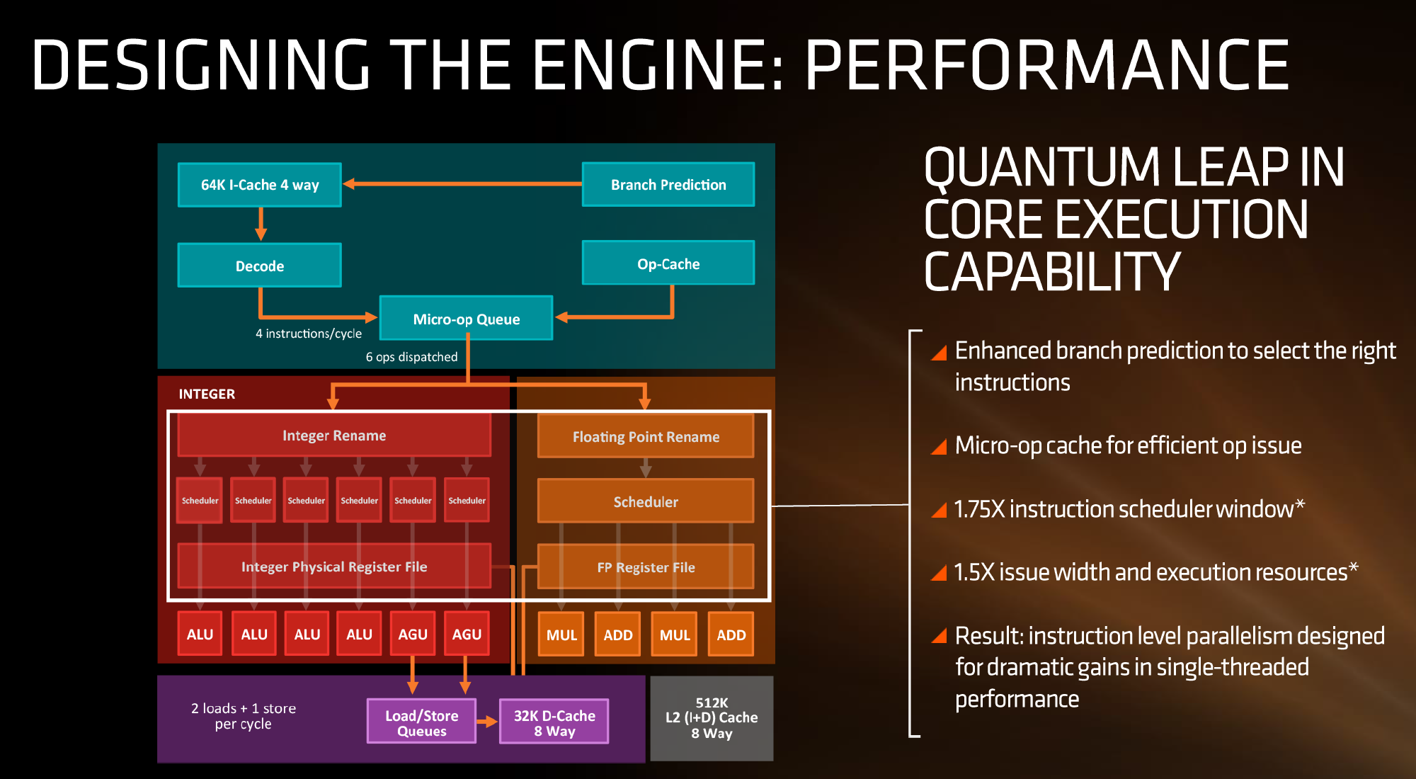
If we focus purely on the left to start, we can see most of the high-level microarchitecture details including basic caches, the new inclusion of an op-cache, some details about decoders and dispatch, scheduler arrangements, execution ports and load/store arrangements. A number of slides later in the presentation talk about cache bandwidth.
Firstly, one of the bigger deviations from previous AMD microarchitecture designs is the presence of a micro-op cache (it might be worth noting that these slides sometimes say op when it means micro-op, creating a little confusion). AMD’s Bulldozer design did not have an operation cache, requiring it to fetch details from other caches to implement frequently used micro-ops. Intel has been implementing a similar arrangement for several generations to great effect (some put it as a major stepping stone for Conroe), so to see one here is quite promising for AMD. We weren’t told the scale or extent of this buffer, and AMD will perhaps give that information in due course.
Aside from the as-expected ‘branch predictor enhancements’, which are as vague as they sound, AMD has not disclosed the decoder arrangements in Zen at this time, but has listed that they can decode four instructions per cycle to feed into the operations queue. This queue, with the help of the op-cache, can deliver 6 ops/cycle to the schedulers. The reasons behind the queue being able to dispatch more per cycle is if the decoder can supply an instruction which then falls into two micro-ops (which makes the instruction vs micro-op definitions even muddier). Nevertheless, this micro-op queue helps feed the separate integer and floating point segments of the CPU. Unlike Intel who uses a combined scheduler for INT/FP, AMD’s diagram suggests that they will remain separate with their own schedulers at this time.
The INT side of the core will funnel the ALU operations as well as the AGU/load and store ops. The load/store units can perform 2 16-Byte loads and one 16-Byte store per cycle, making use of the 32 KB 8-way set associative write-back L1 Data cache. AMD has explicitly made this a write back cache rather than the write through cache we saw in Bulldozer that was a source of a lot of idle time in particular code paths. AMD is also stating that the load/stores will have lower latency within the caches, but has not explained to what extent they have improved.
The FP side of the core will afford two multiply ports and two ADD ports, which should allow for two joined FMAC operations or one 256-bit AVX per cycle. The combination of the INT and FP segments means that AMD is going for a wide core and looking to exploit a significant amount of instruction level parallelism. How much it will be able to depends on the caches and the reorder buffers – no real data on the buffers has been given at this time, except that the cores will have a +75% bigger instruction scheduler window for ordering operations and a +50% wider issue width for potential throughput. The wider cores, all other things being sufficient, will also allow AMD’s implementation of simultaneous multithreading to potentially take advantage of multiple threads with a linear and naturally low IPC.


216 Comments
View All Comments
wumpus - Thursday, August 18, 2016 - link
I want this chip (or a semi-low priced i7 with the graphics removed and 4 more cores in its place) with HBM[2-3] memory (and presumably all the DRAM that fits. Hopefully in 5 years that doesn't imply a transition die) and xpoint as "main memory - SSD buffer/cache/'SSD dram'"So yes, five years at least.
ikjadoon - Thursday, August 18, 2016 - link
No, I think it theoretically is very relevant. If those QD1 numbers are to be believed, we should see noticeable performance increases in day-to-day usage, right?Exactly: it's a fantasy at the price points that are palatable to *consumers*, hehe. Prosumers are also buying $1000+ GPUs, hehe...not the same market.
Right....and that transition is still many years away.
So, what I meant....IDF16 is not very interesting for consumers. AMD timed this presentation quite well.
smilingcrow - Thursday, August 18, 2016 - link
I am not sure that the QD1 numbers will really make a noticeable difference for general consumer usage patterns. Have to wait for real world benchmarks.azazel1024 - Thursday, August 18, 2016 - link
I was very meh about Zen, but now I am actually kind of anticipating it. Even with some of the early engineering sample leaks and rumors that it will be improved IPC, possibly even right up on Skylake, but with much lower clocks. meaning it'll still be lower single threaded performance doesn't bother me too much. BD and it's kin are generally extremely poor single thread compared to Intel's latest Core processors. If Zen comes a fair amount closer...but does it while having 8 cores and 16 threads...that to me says it might actually have a good shot at being in between Skylake/Broadwell and Broadwell-E. If it can do that at a lower price point and being in spitting distance of single thread performance AND manage vaguely reasonable power consumption figures, you could count me as a buyer (if AM4 socketed boards have decent bus support).Give me a Zen with 80-90% of the single thread of Broadwell-E and 80-90% of the mutlthreaded performance of an Octocore Broadwell-E at the price of an entry level Broadwell-E Hexacore, or even a little less ($250-350) and you could count me as a buyer, so long as it isn't some 150TDP monster.
jjj - Thursday, August 18, 2016 - link
Intel rates Broadwell-E at 140W while Zen 8 cores is supposed to be 95W.We'll see about base clocks and Turbo clocks but power might end up being very interesting.
Ofc die size will be interesting too and they should have 4 cores 65W with no GPU.
smilingcrow - Friday, August 19, 2016 - link
Keep in mind that the TDP for the E range tends to be the same for the whole range so in practice the chips below the top of the stack may in reality be capable of using a lower TDP.patel21 - Thursday, August 18, 2016 - link
For me, a performance comparable to i3 skylake, with power requirements at max over 20% of i3, with a good gpu integrated and at around 70% of i3's price. And My boat will sail AMD....Ho yaanandnandnand - Thursday, August 18, 2016 - link
Weren't "8-core" Bulldozer/Excavator chips sold around $200-250? Maybe it's not so crazy to say that AMD will sell Zen real 8-cores in that price range.80% single threaded of Broadwell-E, 80% multithreaded performance, $225. How does that sound?
Gigaplex - Thursday, August 18, 2016 - link
If Zen is much faster than Bulldozer, expect it to cost quite a bit more. Bulldozer sold for peanuts because nobody wanted it.StrangerGuy - Thursday, August 18, 2016 - link
Didn't you already know AMD fanboys have the right to be self-entitled cheapskates?"I want AMD to be competitive but without the competitive price tag along with it because evil Intel/NV."