Ten Year Anniversary of Core 2 Duo and Conroe: Moore’s Law is Dead, Long Live Moore’s Law
by Ian Cutress on July 27, 2016 10:30 AM EST- Posted in
- CPUs
- Intel
- Core 2 Duo
- Conroe
- ITRS
- Nostalgia
- Time To Upgrade
Looking to the Future:
International Technology Roadmap for Semiconductors 2.0
The ten year anniversary of Conroe comes at a time when the International Technology Roadmap for Semiconductors report into the next 10-15 years of the industry has been officially launched to the public. This biennial report is compiled by a group of experts in the semiconductor industry from the US, Europe and Asia and is designed to help the industry dictate which path to focus R&D for the next 10-15 years, and runs for nearly 500 pages. While we could go into extensive detail about the contents, we plan to give a brief overview here. But for people interested in the industry, it’s a great read for sure.
The report includes deep discussions regarding test equipment, process integration, radio frequency implementations (RF), microelectromechanical systems (MEMs), photolithography, factory integration, assembly, packaging, environmental issues, improving yields, modeling/simulation and emerging materials. With a focused path to a number of technologies, the hope is that leading contenders in each part of the industry can optimize and improve efficiency in directional research and development, with the possibility of collaboration, rather than taking many different routes.
Obviously such a report is going to make successful and unsuccessful predictions, even with a group of experts, based on the introduction of moonshot style features (FinFET) or unforeseen limitations in future development. For example, here is the first roadmap published by the Semiconductor Industry Association in the first report in 1993:
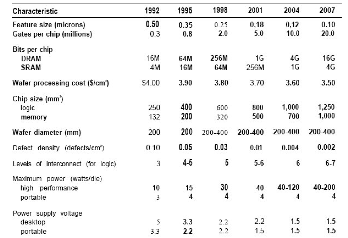
Original 1993 Semiconductor Industry Association roadmap
As we can see, by 2007 it was predicted that we would be on 10nm 100nm chips with up to 20 million ‘gates’, up to 4GB of SRAM per chip and 1250mm2 of logic per die. Up to 400mm wafers were expected in this timeframe, with 200W per die and 0.002 defects per square cm (or 5.65 errors per 300mm wafer).
Compare that to 2016, where we have 16/14nm lithography nodes running 300mm wafers producing 15 billion transistors on a 610mm2 die (NVIDIA P100). Cache currently goes up to 60-65MB on the largest chips, and the power consumption of these chips (the ASIC power) is around 250W as well. So while the predictions were a slow on the lithography node, various predictions about the integration of components onto a base processor were missed (memory controllers, chipsets, other IO).
What makes the most recent report different is that it is listed as the last report planned by ITRS, to be replaced by a more generalized roadmap for devices and systems, the IRDS as the utility of semiconductors has changed over the last decade. In this last report, a number of predictions and focal points have been picked up by the media, indicating a true end to Moore’s Law and how to progress beyond merely shrinking lithography nodes beyond 7nm. Part of this comes from the changing landscape, the move to IoT and the demand for big data processing and storage, but also the decrease in the profitability/performance gain of decreasing node sizes in comparison to their cost to develop is, if believed, set to put a paradigm shift in integrated circuit development. This applies to processors, to mobile, to DRAM and other industry focal points, such as data centers and communications.
I do want to quote one part of the paper verbatim here, as it ties into the fundamental principles of the future of semiconductor engineering:
“Moore’s Law is dead, long live Moore’s Law”
The question of how long will Moore’s Law last has been posed an infinite number of times since the 80s and every 5-10 years publications claiming the end of Moore’s Law have appeared from the most unthinkable and yet “reputedly qualified” sources. Despite these alarmist publications the trend predicted by Moore’s Law has continued unabated for the past 50 years by morphing from one scaling method to another, where one method ended the next one took over. This concept has completely eluded the comprehension of casual observes that have mistakenly interpreted the end of one scaling method as the end of Moore’s Law. As stated before, bipolar transistors were replaced by PMOS that were replaced by NMOS that were also replaced by CMOS. Equivalent scaling succeeded Geometrical Scaling when this could not longer operate and now 3D Power Scaling is taking off.
By 2020-25 device features will be reduces to a few nanometers and it will become practically impossible to reduce device dimensions any further. At first sight this consideration seems to prelude to the unavoidable end of the integrated circuit era but once again the creativity of scientists and engineers has devised a method ‘To snatch victory from the jaws of defeat’.


158 Comments
View All Comments
bcronce - Wednesday, July 27, 2016 - link
My AMD 2500+XP lasted me until a Nahalem i7 2.66ghz. It was a slight.... upgradeartk2219 - Friday, July 29, 2016 - link
Very minor, im sure you barely noticed :).jjpcat@hotmail.com - Wednesday, July 27, 2016 - link
I have a Q6600 in my household and it's still running well.In term on performance, E6400 is about the same as the CPUs (e.g. z3735f/z3745f) used in nearly all cloudbook these days.
Michael Bay - Thursday, July 28, 2016 - link
Yep, I was surprised at that when looking through the benchmarks. Turns out Atom is not so slow after all.stardude82 - Wednesday, July 27, 2016 - link
I've just finished decommissioning all my Core 2 Duo parts, several of which have been upgraded with 2nd hand Sandy Bridge components.Yeah, CPU performance has been relatively stagnant. CPUs have come to where commercial jets are now in their technological development. Jets now fly slower than they did the 1960s, but have much better fuel economy per seat.
Not noted in the E6400 v. i5-6600 comparison is that they both have the same TDP which is pretty impressive. Also, you've got to take inflation into account which would bring the CPU price up to $256 or there about, enough for a i5-6600K.
ScottAD - Wednesday, July 27, 2016 - link
One could argue that while Core put Intel on top of the heap again, Sandy Bridge was a more important shift in design and as a result, many users went from Conroe to Sandy Bridge and have stayed there.That pretty much defines my PC currently. Haven't needed to upgrade. Crazy a decade like nothing.
ianmills - Wednesday, July 27, 2016 - link
When a website has trouble keeping up with current content and instead recycles decades old content.... things that make you go hmm...Ian Cutress - Wednesday, July 27, 2016 - link
I'm the CPU editor, we've been up to date for every major CPU launch for the last couple of years, sourcing units that Intel haven't sourced other websites and have done comprehensive and extensive reviews of every leading x86 development. We have had every Haswell-K (2), Haswell-E(3) Broadwell (2), Broadwell E3 Xeon (3), Broadwell-E (4) and Skylake-K (2) CPU tested and reviewed on each official day of launch. We have covered Kaveri and Carrizo in deep repeated detail over the last few years as well.This is an important chip and today marks in an important milestone.
Hmm...?
smilingcrow - Wednesday, July 27, 2016 - link
Ananand do CPUs very well, can't think of anyone better. Kudos and thanks to you 'guys'."This primarily leaves ARM (who was recently acquired by Softbank)"
They are under offer so not guaranteed to go through and ARM isn't a person. :)
ianmills - Wednesday, July 27, 2016 - link
I agree you do a good job with CPU's. Its some of the other topics that this site has been slowed down in when compared to previous years