Ten Year Anniversary of Core 2 Duo and Conroe: Moore’s Law is Dead, Long Live Moore’s Law
by Ian Cutress on July 27, 2016 10:30 AM EST- Posted in
- CPUs
- Intel
- Core 2 Duo
- Conroe
- ITRS
- Nostalgia
- Time To Upgrade
Looking To The Future: NAND Flash Scales Up to 64 TB SSDs in 2030
Over the past few years, the NAND Flash industry has gone through two major shifts in technology: the movement from 1 to 2 to 3 bits per cell, which directly increases bit density and capacity, and also moving from planar flash to variants of 3D stacking. Stacking can refer to individual NAND dies, as well as stacking those dies into a single package: both of these features are being extensively investigated to increase density also. There are two main drivers for this: reduction in cost, and capacity. However, despite this, the predictions in the ITRS report for NAND flash are primarily looking at improvements to numbers of layers rather than lithography changes or moving to more bits per cell.
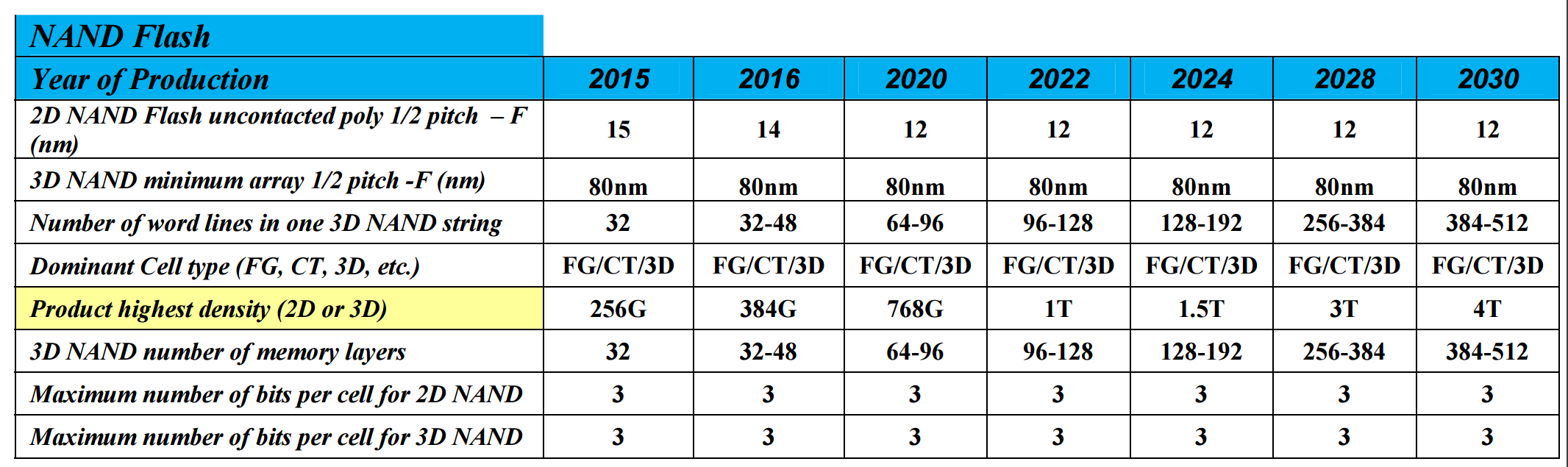
As we can see, TLC (according to the report) is here to stay. QLC, or whatever you want to call it, is not mentioned. The two changes are the number of memory layers, moving from 32 today to 128 around 2022 and then 256/512 by 2030, and the number of word-lines in one 3D NAND string. This gives a product density projection of 256 Gbit packages today to 1 Tbit packages in 2022 and 4 Tbit packages in 2030.
If we apply this to consumer drives available today, we can extrapolate potential SSD sizes for the future. The current Samsung 850 EVO 4 TB uses Samsung’s 48-layer third generation V-NAND to provide 256 Gbit TLC parts. Alongside the 4 TB of memory, the controller requires 4 GB of DRAM, which is another concern to remember. So despite the report stating 256 Gbit in 32-layer, we have 256 Gbit in 48-layer, which is a difference primarily in die-size predictions for the report. Still, if we go off of the product density we should see 12 TB SSDs by 2020, 16 TB in 2022, 48 TB in 2028 and 64 TB drives in 2030. It’s worth noting that the ITRS report doesn’t mention power consumption in this table, nor controller developments which may be a substantial source of performance and/or capacity implementations.


158 Comments
View All Comments
Akrovah - Wednesday, July 27, 2016 - link
My old E6700 is still alive and kicking. I only just replaced it as my primary system when Devil's Canyon came along. Still use it for my four year old's "first computer."djayjp - Wednesday, July 27, 2016 - link
Not a particle physicist, nor electrical engineer, so just some pie in the sky wondering here, but wouldn't it be possible to build transistors using carbon nanotubes, or light itself (using nano sized mirrors/interferometers, like DLP) or even basing the transistor gates off of protons/sub atomic particles?michael2k - Wednesday, July 27, 2016 - link
I think a more interesting question is using glass as a substrate. Imagine printing nand, CPU, GPU, ram, and along the bezels of a smartphone.That reduces a phone to six components: a display, a transducer for sound, a mic, a battery, a radio, and a chassis, which would have all the antennas.
joex4444 - Wednesday, July 27, 2016 - link
Particle physicist here. Light has the tricky property that it travels at the speed of light so I can't imagine it working but perhaps I'm envisioning your concept differently than you are. For carbon nanotubes, you'll need a materials engineer or a condensed matter physicist.3DoubleD - Wednesday, July 27, 2016 - link
Materials/Semiconductor Physics Engineer here. The problem is not what we CAN do, the problem is what is economically possible at scale. For example, FinFETs were demonstrated at the turn of the century, but took all of those years to become (1) necessary - planar transistor were getting too leaky, and (2) possible to fabricate economically in large scales.Researchers have created smaller, faster transistors years ago, but it takes a lot of time and effort to develop the EUV or quadruple patterning technologies that enable these devices to be reliably and affordably manufactured.
So I think the problem in moving "beyond silicon" is not that we don't have alternatives, it is that we have many alternatives, we just don't know which will scale. It becomes less of a purely engineering problem and manufacturing business problem. When new technologies relied purely on the established silicon industry alone, you could reasonably extrapolate how much each new technology would cost as the nodes were scaled down. When we talk about using III-V FinFETs/ All Around Gates or graphene and carbon nanotubes, we don't really know how those things will scale with the existing processes as we move them from the laboratory to the manufacturing line.
I've been looking forward to this transition for years. People moan that it is the end of Moores Law, but that could be a good thing. Silicon is a great material for forming logic circuits for many reasons, but it also has many downsides. While silicon never reached 10 GHz (as Intel once predicted), other materials easily blow past 100 GHz transistor switching speeds. When the massive engines that work tirelessly to reduce our lithography nodes nm by nm are aimed at "the next big thing", we might be pleasantly surprised by a whole new paradigm of performance.
So what competes with modern day Si CMOS on speed, power usage, and cost? Nothing... yet!
djayjp - Thursday, July 28, 2016 - link
Yes, it's fascinating stuff. Thanks for reminding me about that. I recall now that I think it was graphene that enabled those insanely high switching speeds, due to its incredible conductivity/efficiency. Hopefully it can now be made economically feasible at some point! Imagine a the next GPU that is 10x smaller and operates at 100x the clock speed. A GTX 1080Ti x 1000! Finally we can do real time true global illumination ha....jeffry - Monday, August 1, 2016 - link
Thats a good point. Like, answering a question "are you willing to pay $800 for a new CPU to double the computers speed?" Most consumers say no. It all comes down to the mass market price.wumpus - Thursday, August 4, 2016 - link
From the birth of the Univac until 10 years ago, consumers consistently said YES! and plunked down their money. Doubling the (per thread) speed of a core2duo is going to cost more than $800. Also the cost of the RAM on servers is *WAY* more than $800, so you can expect if Intel could double the power of each core, they could crank prices up by at least $800 per core on Xeons. They can't, and neither can IBM or AMD.Jaybus - Thursday, July 28, 2016 - link
Sure, but that speed is dependent on the medium. There are some proposed optical transistors using electromagnetically induced transparency. Long way off. However, silicon photonics could change some things. Capacitance is the killer for electronic interconnects, whether chip-to-chip or on-chip bus. An optical interconnect could greatly increase bandwidth without increasing the chip's power dissipation. I think an electronic-photonic hybrid is more likely, since silicon photonics components can be made on a CMOS process. We are already beginning to see optical PCI Express being deployed. I could definitely see a 3D approach where 2D electronic layers are connected through an optical rather than electronic bus.djayjp - Thursday, July 28, 2016 - link
Yes, transparency, like polarized windows that either become transparent or opaque when a current is applied (to the liquid crystals?). I wonder how small they could be made. It would be incredibly power efficient I would think.