Ten Year Anniversary of Core 2 Duo and Conroe: Moore’s Law is Dead, Long Live Moore’s Law
by Ian Cutress on July 27, 2016 10:30 AM EST- Posted in
- CPUs
- Intel
- Core 2 Duo
- Conroe
- ITRS
- Nostalgia
- Time To Upgrade
Looking To The Future: NAND Flash Scales Up to 64 TB SSDs in 2030
Over the past few years, the NAND Flash industry has gone through two major shifts in technology: the movement from 1 to 2 to 3 bits per cell, which directly increases bit density and capacity, and also moving from planar flash to variants of 3D stacking. Stacking can refer to individual NAND dies, as well as stacking those dies into a single package: both of these features are being extensively investigated to increase density also. There are two main drivers for this: reduction in cost, and capacity. However, despite this, the predictions in the ITRS report for NAND flash are primarily looking at improvements to numbers of layers rather than lithography changes or moving to more bits per cell.
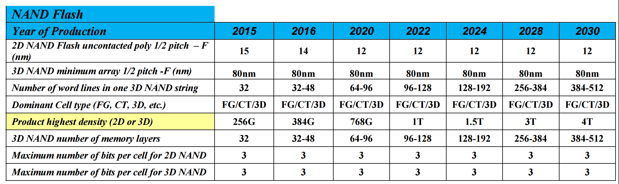
As we can see, TLC (according to the report) is here to stay. QLC, or whatever you want to call it, is not mentioned. The two changes are the number of memory layers, moving from 32 today to 128 around 2022 and then 256/512 by 2030, and the number of word-lines in one 3D NAND string. This gives a product density projection of 256 Gbit packages today to 1 Tbit packages in 2022 and 4 Tbit packages in 2030.
If we apply this to consumer drives available today, we can extrapolate potential SSD sizes for the future. The current Samsung 850 EVO 4 TB uses Samsung’s 48-layer third generation V-NAND to provide 256 Gbit TLC parts. Alongside the 4 TB of memory, the controller requires 4 GB of DRAM, which is another concern to remember. So despite the report stating 256 Gbit in 32-layer, we have 256 Gbit in 48-layer, which is a difference primarily in die-size predictions for the report. Still, if we go off of the product density we should see 12 TB SSDs by 2020, 16 TB in 2022, 48 TB in 2028 and 64 TB drives in 2030. It’s worth noting that the ITRS report doesn’t mention power consumption in this table, nor controller developments which may be a substantial source of performance and/or capacity implementations.


158 Comments
View All Comments
saratoga4 - Wednesday, July 27, 2016 - link
>As we can see, by 2007 it was predicted that we would be on 10nm chipsShould be 100 nm (0.1 microns).
Jehab - Wednesday, July 27, 2016 - link
Yeah, that is a massive error, lol.hammer256 - Wednesday, July 27, 2016 - link
If I remember correctly, intel was running at 65nm in 2007 right? So I guess that was ahead of the curve at the time.JlHADJOE - Saturday, July 30, 2016 - link
And the 2001 ITR roadmap actually predicted 22nm for 2016. Despite the delays getting to 14/16nm the industry is actually way ahead of the curve.http://www2.lbl.gov/Science-Articles/Archive/ALS-E...
melgross - Wednesday, July 27, 2016 - link
Exactly! I was going to post that myself. Once it's understood that it's actually 100nm, the other numbers make sense, otherwise, they don't.Walkermoon - Wednesday, July 27, 2016 - link
Just signed up to say the same.Ian Cutress - Wednesday, July 27, 2016 - link
Derp, I misread the table in a rush. Updated.Pissedoffyouth - Wednesday, July 27, 2016 - link
Could you bench it against an AMD A10 Kaveri? That would be goodGc - Saturday, July 30, 2016 - link
AMD A10-7800 (Kaveri) is in three of the bar charts on page 6. It appears to benefit from 4 cores in two of the comparisons.Zaxx420 - Wednesday, July 27, 2016 - link
Still have a E8400 rig that I use every day...with it o/ced to 4GHz, 8gb of DDR2-1066 and a OCZ Vertex 2 SSD plus it's 6mb of cache on a P45 mobo...it can hold its own to this day...easily. The E8000 series is one of the best 'future proof' cpus ever...next up imo will prove to be Sandy Bridge. Have a 2500K at 4.5GHz on a Z68 mobo, 16gb DDR3-2400 and a Samsung 850 Pro ssd...and now a GTX 1060...plays any game I want at 1080 and max quality...easily.