Ten Year Anniversary of Core 2 Duo and Conroe: Moore’s Law is Dead, Long Live Moore’s Law
by Ian Cutress on July 27, 2016 10:30 AM EST- Posted in
- CPUs
- Intel
- Core 2 Duo
- Conroe
- ITRS
- Nostalgia
- Time To Upgrade
Looking To The Future: 450mm Wafers in 2021, and Down to ‘2nm’
Most users following the industry will know that the name of the lithographic node, such as ‘14nm’, ‘16nm’ or ‘28nm’ is often an imperfect characterization of what is actually happening on the silicon. For example, Intel’s 14nm node is widely touted as the best in the industry, and the equivalent 14nm/16nm nodes are said to not be even close, due to Intel’s focus on several generations of FinFET compared to the other main semiconductor manufacturers. This also means that while ‘14nm’ or ‘16nm’ is mentioned, many other parts of the silicon could be manufactured on other nodes, depending on the utility.
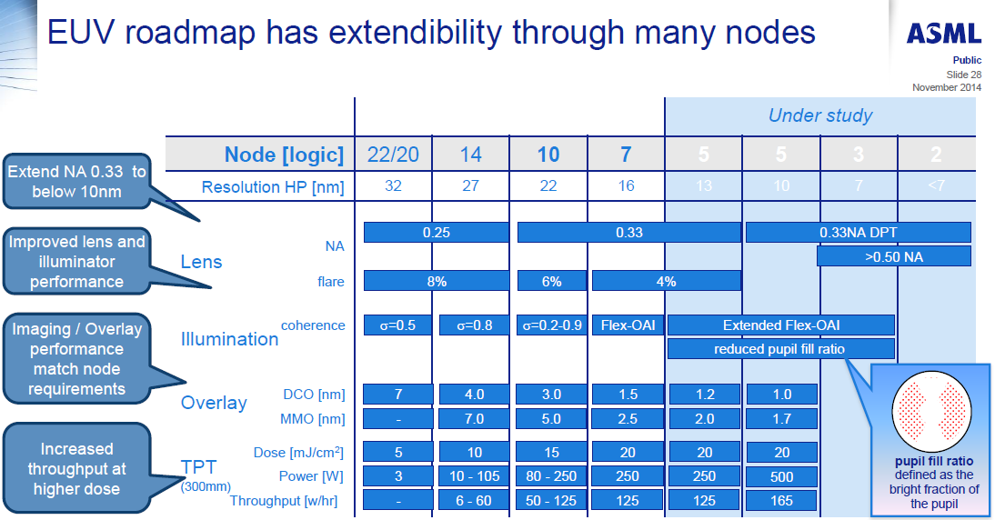
We’ve spoken in the past about equipment roadmaps to deal with the problem of shrinking lithography node sizes. This includes new lasers, droplet generation, collectors, masks, defect detection, lenses, and the technology to drive high throughput. For example, here are ASML’s EUV requirements for the next few manufacturing nodes, including requirements for 250W light sources at a 5nm node:
With the ITRS report, it makes a couple of metrics regarding node sizes and wafers. On the later, we get the prediction that 450mm wafers should be in play at around 2021 for DRAM:
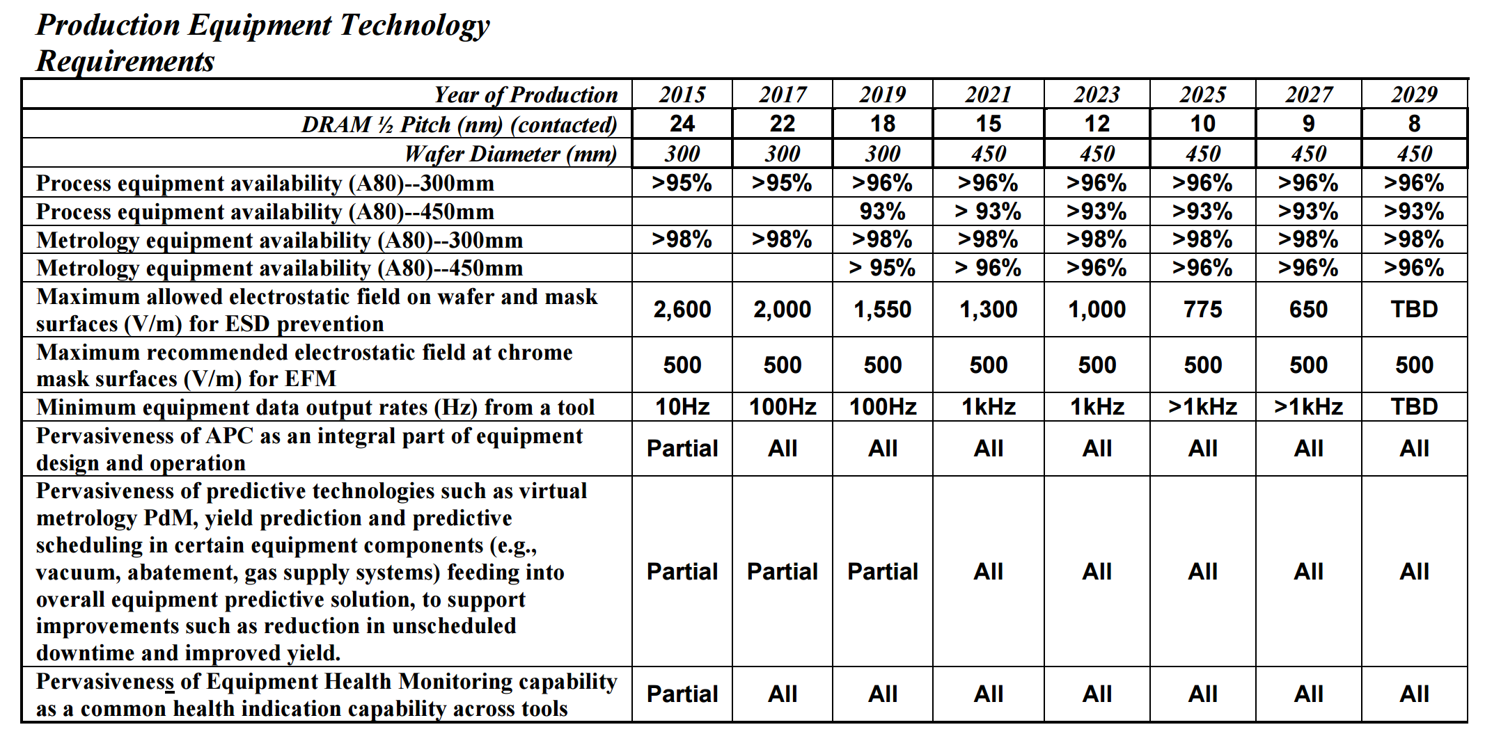
This matches at DRAM half-pitch of 15nm, or a DRAM cell size of 780nm2, compared to 3480nm2 today. The movement to 450mm wafers has been expected for some time, with early predictions going for the 2008-2011 timeframe, however development seems to have stalled for a variety of reasons.
When it comes to transistors, given the node naming scheme caveats listed above, the ITRS report predicts that FinFET will make way at around the 2021 timeframe in favor of 3D stacking such as ‘vertical gate all-around’ (VGAA). As the node shrinks, as well as the transistor size, the power supply voltage will drop from 800mV today down to 400/450mV by 2027.
![]()
Moving into a world of IoT will require even lower power transistors, of which moving to a ‘smaller node’ and vertical chip integration will be a large part.
The ITRS report goes into a lot of detail regarding different stacking technologies, such as the 2.5D integration we see on products like AMD’s Fiji GPU involving a silicon interposer, as well as 3D and the different ways to implement both microchannel cooling in such chips as well as 3D TSV applications.


158 Comments
View All Comments
saratoga4 - Wednesday, July 27, 2016 - link
>As we can see, by 2007 it was predicted that we would be on 10nm chipsShould be 100 nm (0.1 microns).
Jehab - Wednesday, July 27, 2016 - link
Yeah, that is a massive error, lol.hammer256 - Wednesday, July 27, 2016 - link
If I remember correctly, intel was running at 65nm in 2007 right? So I guess that was ahead of the curve at the time.JlHADJOE - Saturday, July 30, 2016 - link
And the 2001 ITR roadmap actually predicted 22nm for 2016. Despite the delays getting to 14/16nm the industry is actually way ahead of the curve.http://www2.lbl.gov/Science-Articles/Archive/ALS-E...
melgross - Wednesday, July 27, 2016 - link
Exactly! I was going to post that myself. Once it's understood that it's actually 100nm, the other numbers make sense, otherwise, they don't.Walkermoon - Wednesday, July 27, 2016 - link
Just signed up to say the same.Ian Cutress - Wednesday, July 27, 2016 - link
Derp, I misread the table in a rush. Updated.Pissedoffyouth - Wednesday, July 27, 2016 - link
Could you bench it against an AMD A10 Kaveri? That would be goodGc - Saturday, July 30, 2016 - link
AMD A10-7800 (Kaveri) is in three of the bar charts on page 6. It appears to benefit from 4 cores in two of the comparisons.Zaxx420 - Wednesday, July 27, 2016 - link
Still have a E8400 rig that I use every day...with it o/ced to 4GHz, 8gb of DDR2-1066 and a OCZ Vertex 2 SSD plus it's 6mb of cache on a P45 mobo...it can hold its own to this day...easily. The E8000 series is one of the best 'future proof' cpus ever...next up imo will prove to be Sandy Bridge. Have a 2500K at 4.5GHz on a Z68 mobo, 16gb DDR3-2400 and a Samsung 850 Pro ssd...and now a GTX 1060...plays any game I want at 1080 and max quality...easily.