Ten Year Anniversary of Core 2 Duo and Conroe: Moore’s Law is Dead, Long Live Moore’s Law
by Ian Cutress on July 27, 2016 10:30 AM EST- Posted in
- CPUs
- Intel
- Core 2 Duo
- Conroe
- ITRS
- Nostalgia
- Time To Upgrade
Looking To The Future: NAND Flash Scales Up to 64 TB SSDs in 2030
Over the past few years, the NAND Flash industry has gone through two major shifts in technology: the movement from 1 to 2 to 3 bits per cell, which directly increases bit density and capacity, and also moving from planar flash to variants of 3D stacking. Stacking can refer to individual NAND dies, as well as stacking those dies into a single package: both of these features are being extensively investigated to increase density also. There are two main drivers for this: reduction in cost, and capacity. However, despite this, the predictions in the ITRS report for NAND flash are primarily looking at improvements to numbers of layers rather than lithography changes or moving to more bits per cell.
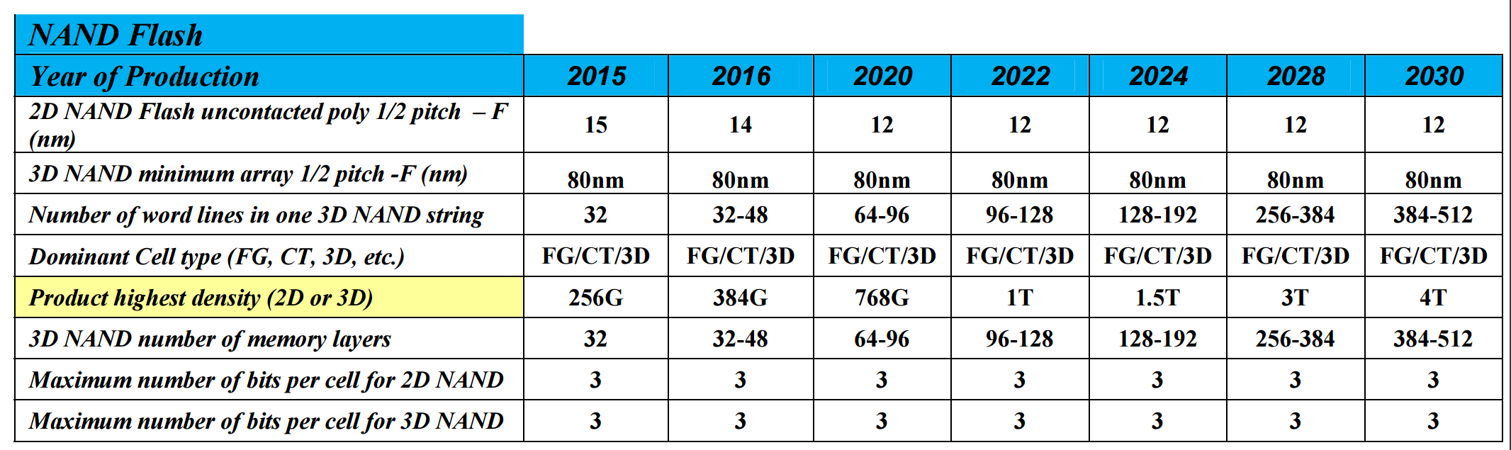
As we can see, TLC (according to the report) is here to stay. QLC, or whatever you want to call it, is not mentioned. The two changes are the number of memory layers, moving from 32 today to 128 around 2022 and then 256/512 by 2030, and the number of word-lines in one 3D NAND string. This gives a product density projection of 256 Gbit packages today to 1 Tbit packages in 2022 and 4 Tbit packages in 2030.
If we apply this to consumer drives available today, we can extrapolate potential SSD sizes for the future. The current Samsung 850 EVO 4 TB uses Samsung’s 48-layer third generation V-NAND to provide 256 Gbit TLC parts. Alongside the 4 TB of memory, the controller requires 4 GB of DRAM, which is another concern to remember. So despite the report stating 256 Gbit in 32-layer, we have 256 Gbit in 48-layer, which is a difference primarily in die-size predictions for the report. Still, if we go off of the product density we should see 12 TB SSDs by 2020, 16 TB in 2022, 48 TB in 2028 and 64 TB drives in 2030. It’s worth noting that the ITRS report doesn’t mention power consumption in this table, nor controller developments which may be a substantial source of performance and/or capacity implementations.


158 Comments
View All Comments
Ian Cutress - Tuesday, August 2, 2016 - link
To clarify, there was a typo in Johan's original review of the microarchitecture, specifically stating:'However, Core is clearly a descendant of the Pentium Pro,'
I've updated the article to reflect this, and was under the assumption that my source was correct at the point of doing my research.
wumpus - Tuesday, August 2, 2016 - link
Except that the Pentium Pro was the first chip with the P6 architecture. Pentium 2 was pretty much pentium pro with MMX, a higher clock rate, and slower [off chip but on slot] L2 cache. Pentium 3 was the same with more clock, more MMX (possibly SSE), and on chip (full speed) L2 cache.While I'd have to assume they would pull all the files from the Pentium 3 plans, I'd still call it "pentinium pro based" because that was where nearly all the architecture came from (with minor upgrades and bug fixes to the core in 2 and 3).
I'm still curious as to exactly how they pulled it off. My main theory is that they duplicated the block diagram of the P6, and then verified each block was correct (and exactly duplicated the P6 at a higher speed), then used the P6 verification to prove that if the blocks were all correct, they had a correct chip.
zodiacfml - Thursday, July 28, 2016 - link
Same here. I thought it was the design of the Pentium M (from Israel team) they got the Core from. It was that time that AMD is beating Intel's P4's in performance, efficiency, and price. After a few months, articles were posted with people able to overclock a Pentium M with the characteristics of the AMD CPU and, of course, beating Pentium 4's at much lower clock speeds. From there, the Intel Core was born out of the Pentium M's which is essentially the same only with higher TDP and clock speeds. Then came, the Core Duo, then the Core 2 Duo.I just can't remember where I read it though.
marty1980 - Wednesday, July 27, 2016 - link
I started college in electrical engineering; moved to software after an ee class using c++. I was very excited and confident in a DIY PC. I knew the Core 2 was on its way. I gathered parts from whatever computers I could scratch together; power supply, case, DVD drive, network card(s), HDDs ... Everything but Mobo, CPU, GPU and RAM - the brains.I bought an E6400 2.13GHz with a gigabyte mobo, 4GB 800MHz DDR2 and a Radeon x1650 Pro.
I just retired the CPU and Mobo in 2012/13 when I experimented with my current PC; an AMD APU + Ded GPU (dual graphics).
I'm excited to be looking at a future replacement for my PC. We're on the horizon of some interesting changes that I don't even understand (what was his article about? Lol).
just4U - Thursday, July 28, 2016 - link
I seem to recall from a casual glance at an article (on this site) back some 9 years ago.. That intel basically got lucky, or fluked as it were.. Something to do with what they were doing with the PentiumM which caused them to move away from the P3-4 stuff.. hum.. damned if I can remember though what it was about.FourEyedGeek - Tuesday, August 9, 2016 - link
Pentium 3 architecture was having difficulties increasing performance so they replaced it with Pentium 4s Netburst. They had their Israel department continue work on Pentium 3 that turned into the Pentium M.Hazly79 - Thursday, July 28, 2016 - link
surprised that my 2005-Pentium D 3ghz still can run Diablo 3 (2012) at minimum setting pair with Nvidia GT 710 ($35 card )Really great optimization from Blizzard ent. team...
AnnonymousCoward - Thursday, July 28, 2016 - link
Yeah, but too bad the game sucks. Jay doubled it.name99 - Thursday, July 28, 2016 - link
Two points:Firstly macro-op fusion is hardly an x86 exclusive these days. Many (all?) ARMv8 CPUs use it, as do the most recent POWER CPUs. Like the x86 case, it's used to fuse together pairs of instructions that commonly co-occur. Compare and branch is a common example, but other common examples in RISC are instruction pairs that are used to create large constants in a register, or to generate large constant offsets for loads/stores.
Secondly you suggest that the ROB is an expensive data structure. This is misleading. The ROB itself is primarily a FIFO and can easily be grown. The problem is that storing more items in the ROB requires more physical registers and more load/store queue entries, and it is THESE structures that are difficult and expensive to grow. This suggests that using alternative structures for the load/store queues, and alternative mechanisms for scavenging physical registers could allow for much larger ROBs, and in fact Intel has published a lot of work on this (but has so far done apparently nothing with this research, even though the first such publications were late 90s --- I would not be surprised if Apple provides us with a CPU implementing these ideas before Intel does).
Ian Cutress - Tuesday, August 2, 2016 - link
It wasn't written about to the exclusion of all other microarchitectures, it was written about focusing on x86 back in 2006. At the time, the ROB was described as expensive by Intel, through I appreciate that might have changed.