Ten Year Anniversary of Core 2 Duo and Conroe: Moore’s Law is Dead, Long Live Moore’s Law
by Ian Cutress on July 27, 2016 10:30 AM EST- Posted in
- CPUs
- Intel
- Core 2 Duo
- Conroe
- ITRS
- Nostalgia
- Time To Upgrade
Looking To The Future: NAND Flash Scales Up to 64 TB SSDs in 2030
Over the past few years, the NAND Flash industry has gone through two major shifts in technology: the movement from 1 to 2 to 3 bits per cell, which directly increases bit density and capacity, and also moving from planar flash to variants of 3D stacking. Stacking can refer to individual NAND dies, as well as stacking those dies into a single package: both of these features are being extensively investigated to increase density also. There are two main drivers for this: reduction in cost, and capacity. However, despite this, the predictions in the ITRS report for NAND flash are primarily looking at improvements to numbers of layers rather than lithography changes or moving to more bits per cell.
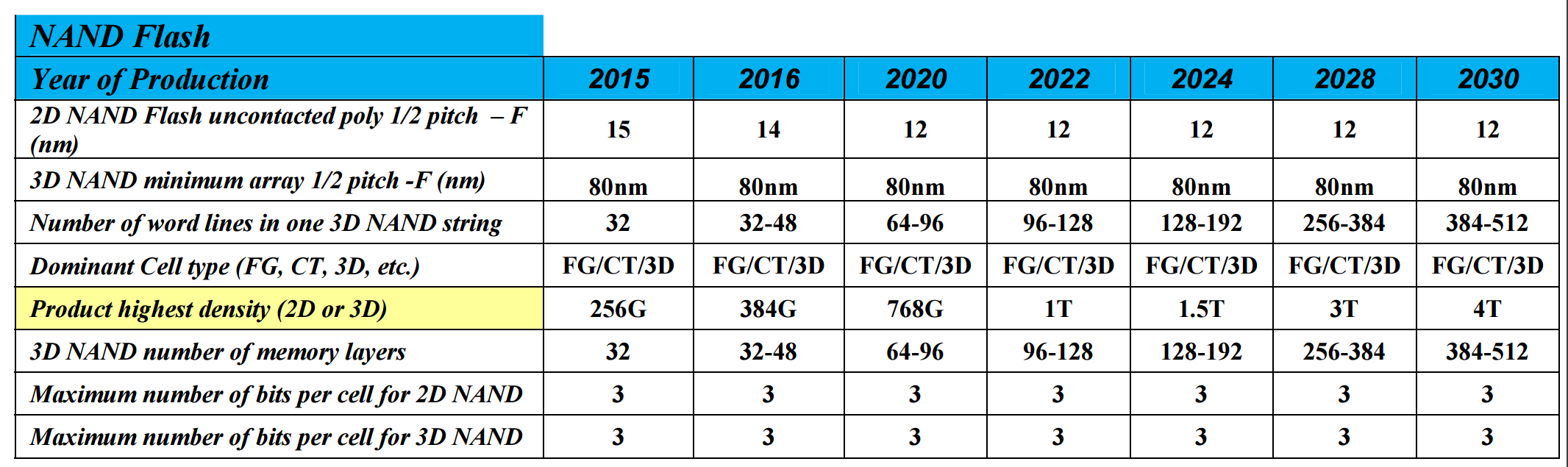
As we can see, TLC (according to the report) is here to stay. QLC, or whatever you want to call it, is not mentioned. The two changes are the number of memory layers, moving from 32 today to 128 around 2022 and then 256/512 by 2030, and the number of word-lines in one 3D NAND string. This gives a product density projection of 256 Gbit packages today to 1 Tbit packages in 2022 and 4 Tbit packages in 2030.
If we apply this to consumer drives available today, we can extrapolate potential SSD sizes for the future. The current Samsung 850 EVO 4 TB uses Samsung’s 48-layer third generation V-NAND to provide 256 Gbit TLC parts. Alongside the 4 TB of memory, the controller requires 4 GB of DRAM, which is another concern to remember. So despite the report stating 256 Gbit in 32-layer, we have 256 Gbit in 48-layer, which is a difference primarily in die-size predictions for the report. Still, if we go off of the product density we should see 12 TB SSDs by 2020, 16 TB in 2022, 48 TB in 2028 and 64 TB drives in 2030. It’s worth noting that the ITRS report doesn’t mention power consumption in this table, nor controller developments which may be a substantial source of performance and/or capacity implementations.


158 Comments
View All Comments
Hazly79 - Wednesday, July 27, 2016 - link
History of Intel processori 386 1986
i 486 1989 - 94
Pentium / MMX 1994 - 96
Pentium II 1997
Pentium III 1999
Pentium 4 / 4 HT 2002 - 04
Pentium D 2005
Core [ 2 ] Duo 2006 - 08
Core [ 2 ] Quad 2007 - 08
Core [ i ] Nehalem 2008
Core [ i ] Westmere 2009
Core [ i ] Sandy Bridge 2011
Core [ i ] Ivy Bridge 2012
Core [ i ] Haswell 2013
Core [ i ] Broadwell 2014
Core [ i ] Skylake 2015
Core [ i ] Kabylake 2016
AnnonymousCoward - Wednesday, July 27, 2016 - link
So how many decades will it take til cpus have significantly faster single-thread than a 6700K@4.4GHz?Notmyusualid - Thursday, July 28, 2016 - link
+1Mr Perfect - Wednesday, July 27, 2016 - link
Hmm. We've got an ancient 2007 Macbook with a 2GHz C2D(T7200 I think) in it that's still used for web browsing on a daily basis. Upgrading it to 4GB of ram and a SSD made it surprisingly capable.It's not all a bed of roses though, as random things will come out of left field and floor it. I think it's mostly flash heavy sites, but Twitter and Vine freak it out a little.
Hulk - Wednesday, July 27, 2016 - link
I vividly remember the anticipation and hype leading up to the C2D release. The the years of struggle Intel had with Netburst before Conroe. It was what I consider the end of the golden age of the CPU. Great job Ian!Impulseman45 - Wednesday, July 27, 2016 - link
Ah, it wasn't the Pentium Pro it was based on. The Core family was a direct descendant of the Pentium 3 Tualatin. They stopped sales of the of the Pentium 3 Tualatin because it was outperforming the Pentium 4. They migrated that technology to the notebook line as it was much more efficient. It became the Pentium M. When Intel realized that the Pentium 4 Netburst architecture was a dead end and they needed a new chip to go up against AMD, they sourced their notebook chips to build the Core series. See this is what is called re-writing history. Come on guys, it is very well known that they sourced the Pentium M Yohan for the Core series. I do not know who did your research but it is all wrong. Go back and recheck your information. The Pentium Pro was the granddaddy of all the Pentium 2 and 3 chips so yeah, you can point to that chip in a vague way as the ancestor. But the Pentium 4 can as well well. So to be to the point, the core lines DNA goes back directly to the Pentium 3 Tualatin, So we have all been using very, very hopped up Pentium 3s the last 10 years. The Tualatin was an excellent chip. It overclock like crazy. There were Celeron and Sever P3 versions and all of them beat the hell out of the P4. Its know reason Intel had to kill it. Do more research so you can post accurate articles, please.Michael Bay - Thursday, July 28, 2016 - link
>teaching AT about CPU architecturesDamn it, you`re a riot!
Impulseman45 - Thursday, July 28, 2016 - link
These are not the original AT guys, they are all new people and they are not doing the research they should be doing. This is how history can get changed. People look to a reputable tech site that got something wrong and its written in stone. Well AT says this is how it is, even if they are wrong. Go check the history directly from Intel, This article is wrong and that is a fact, period. I felt it just needed to be called out on.natenu - Monday, August 1, 2016 - link
Refreshing to see this comment. HT was a marketing joke to keep up with clock rate shoppers.wumpus - Tuesday, August 2, 2016 - link
When Dave Barry jokes about "speed is measured in Megahertz" you know you are ripe for some marketing in your engineering.