The GIGABYTE Z170X-UD5 TH Motherboard Review: An Entry to Thunderbolt 3
by Ian Cutress on February 19, 2016 9:00 AM EST- Posted in
- Motherboards
- Gigabyte
- Thunderbolt
- Skylake
- Z170
- Thunderbolt 3
GIGABYTE Z170X-UD5 TH BIOS
A proportion of this page was posted with our GIGABYTE Z170X-Gaming G1 review due to similarities within the same generation of products. Text has been updated to match the specific features for this review.
The graphical BIOS has been a permanent competitive fixture in the modern motherboard market – the ability to do more with less and provide a seamless experience to both enthusiasts and new users is a point that manufacturers can provide both a selling point and that unique aspect that makes it stand above the crowd. The big four motherboard manufacturers have now all adopted the same philosophy of an easier mode for a front screen that sits above an Advanced mode which is more enthusiast focused.


While GIGABYTE does typically have an easy mode, called the startup guide, with its motherboards, for the Z170X-UD5 TH it was absent and we were left solely with the classic mode. With this mode, it should be pointed out that sometimes there is a disjoint when you enter between what you see and what the system thinks is selected – about 50% of the time it will show the first tab, MIT, rather than the one which is actually selected, System Information. Pressing left or right to select a tab usually fixes this.
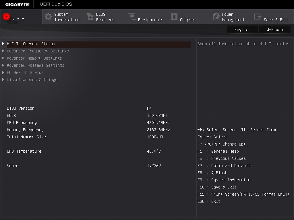
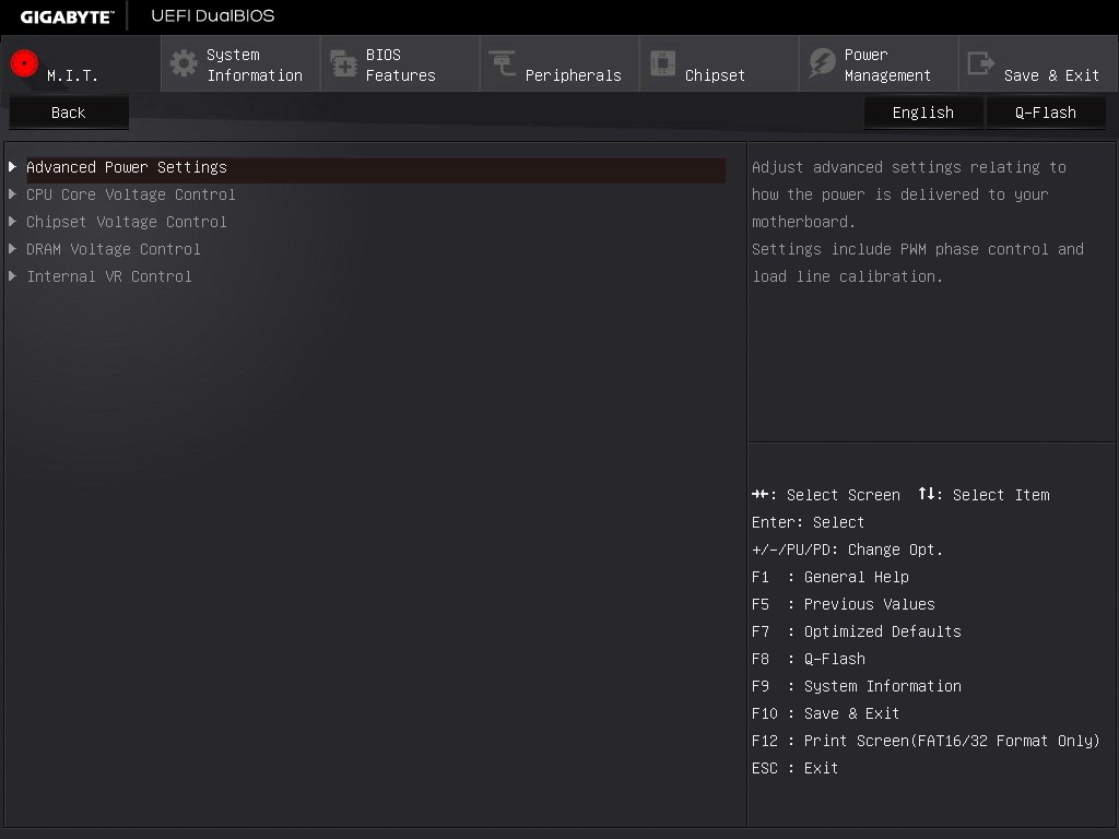
The first tab from the left is MIT, the intelligent tweaking menu that provides some information about the system but acts as the main hub for overclocking options. The three main menus here are Frequency, Memory and Voltage, which all do what they say and offer options relating to those features.
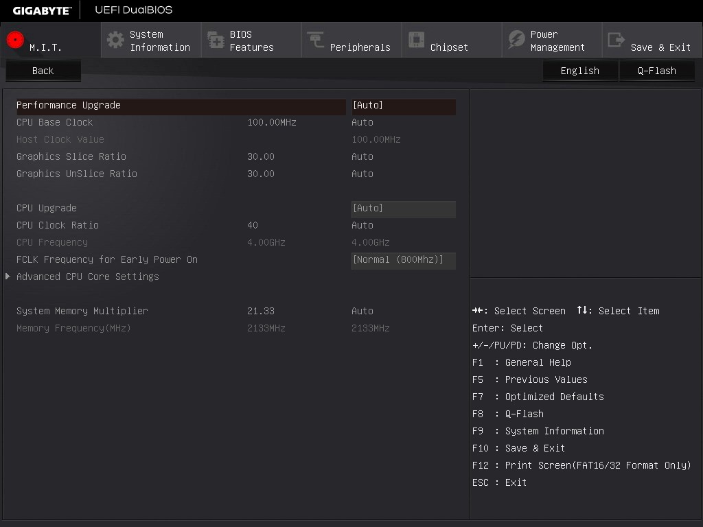
The Frequency sub-menu offers base-clock and multiplier options for the CPU, including FCLK and advanced core settings. For an extra element, the DRAM multiplier can be selected here also, such that as the base frequency is adjusted the user can see the effect on the memory frequency. Automatic overclock pre-sets are also here under the Performance Upgrade drop down and the CPU Upgrade drop down.
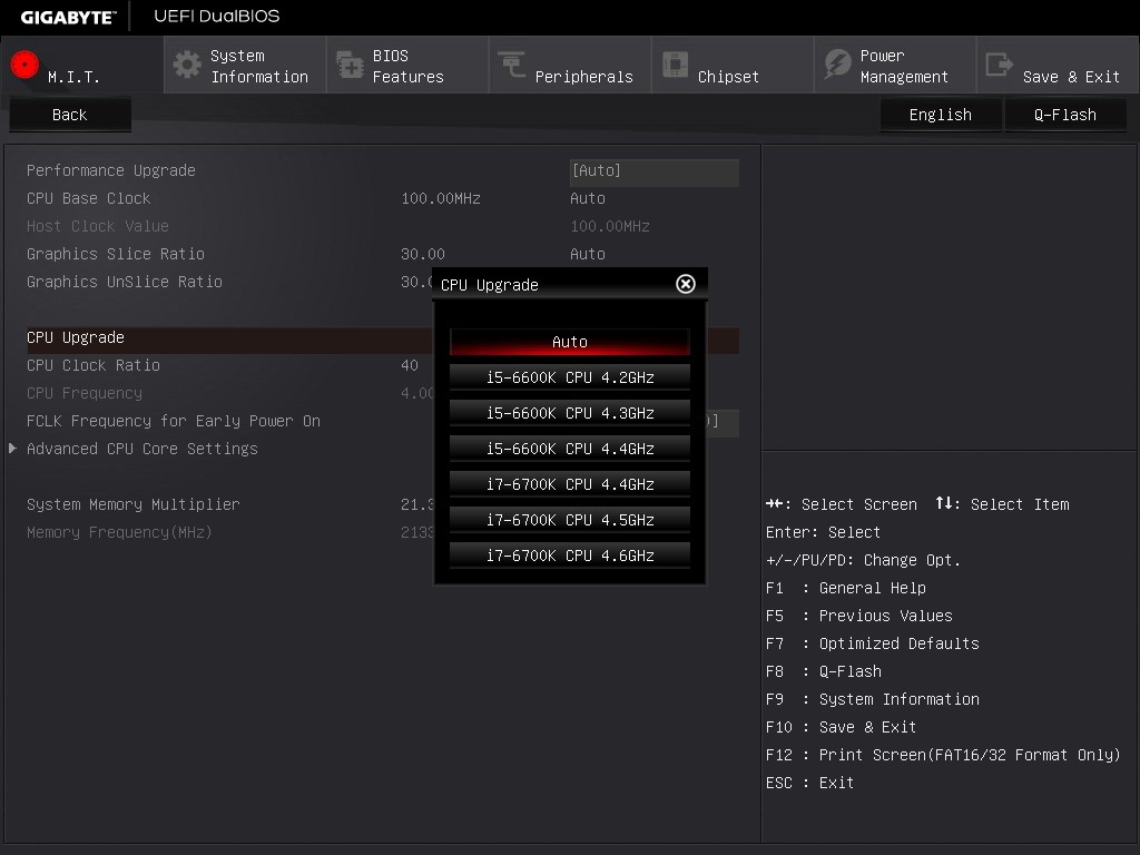
This latter option offers 4.2 GHz to 4.4 GHz for the i5-6600K and 4.4 GHz to 4.6 GHz for the i7-6700K. The downsides of using these options is that GIGABYTE doesn’t show the changes made to enable these (such as voltage or LLC), in which GIGABYTE is unique in that regard compared to the others of the big four manufacturers.
In our previous reviews, it was noted that a typical overclocker will want to adjust frequency and voltage often in the same sitting. With the GIGABYTE BIOS, that requires moving into this frequency menu for the first part, and navigating to different menus for the voltage. It would be ideal if the GIGABYTE BIOS duplicated some of those options, at least the CPU vCore and CPU Load-Line Calibration, to the frequency menu just as the memory multiplier has been duplicated.
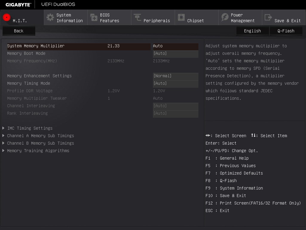
The Memory sub-menu gives options to enable XMP, adjust memory sub-timings but also implement a form of memory enhancement. To the best of my abilities, this seems to be an option that adjusts a number of tertiary sub-timings that might affect certain workflows. As with any overclocking, this is not guaranteed and your mileage may vary.
The Voltage sub-menu actually opens another set of sub-menu options, including power, core voltage and DRAM voltage. We’ve spoken to GIGABYTE about their method of doing it this way in the past, and the answer is to make options easier to find by separating them out – personally some of these options could be joined up and still fit on screen very easily, such as a ‘simple’ and ‘advanced’ voltage sub-menu that provides some options duplicated but the simple set is just the few that most overclockers will want to use.
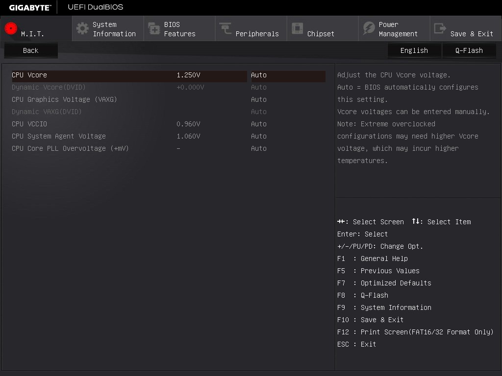
Nevertheless we find the processor load line calibration in the power settings menu, the processor voltage (CPU, GPU, Ring and PLL) in the Core Voltage Control, memory voltage in the DRAM menu and anyone extreme enough to enter the voltage regulation control can go nuts, with plenty of options that few engineers understand.
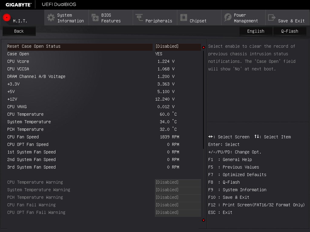
The MIT tab also offers a PC Health menu which contains all the sensor readings as well as the fan controls.
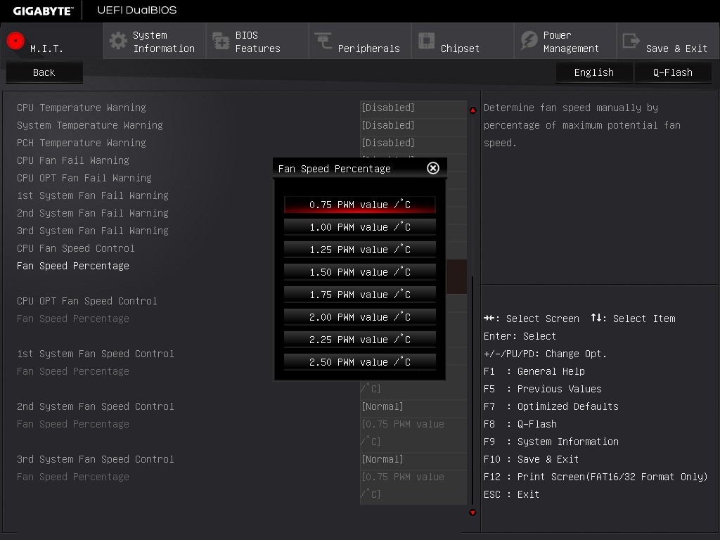
GIGABYTE is still lacking an interactive fan control option in the BIOS, while the other manufacturers have such a system with several points users can modify with a mouse. Instead from GIGABYTE we have a series of options relating to PWM/°C, which is a confusing metric if you do not understand fans. To explain it, basically the system can apply a value of 0 PWM to 255 PWM to the fan which relates to the fan voltage. This scale is not always linear, and what makes it frustrating is that the fan’s response is also non-linear to the voltage applied. Technically GIGABYTE could detect the fan RPM as a function of PWM and do the mathematics to provide gradients with actual RPM values, but instead we get basic PWM values. Just to put it into context, some fans are at 0 RPM until 40% PWM (40% of 255 is 102), and then shoot to 60% of their peak RPM speed. So at a gradient of 1 PWM value per degree, you would only see the fan turn on at 102 degrees, which by then it’s too late as the machine might have shut down due to overheating. Fan speed control is a very easy concept to fix, but for whatever reason is left like this.
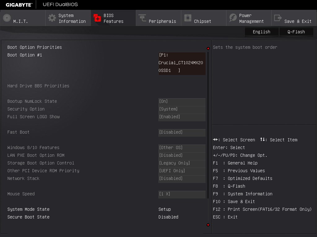
After MIT, the next important tab is the BIOS Features one which allows boot sequence adjustments as well as fast boot, Windows 10 and secure boot options. A newer option here is the Mouse Speed option, designed to assist mouse movement in the BIOS.
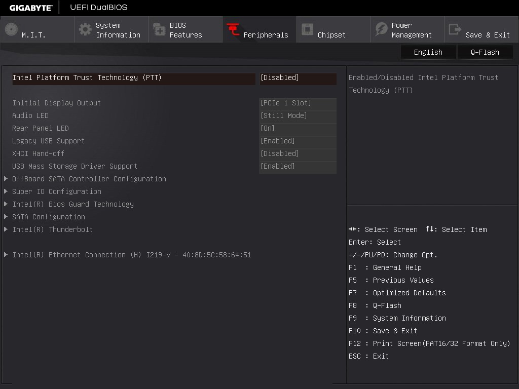
The Peripherals tab is where the extra controllers can be adjusted as well as the LED lighting, SATA Controller configuration (AHCI/RAID), NVMe support and Thunderbolt support.
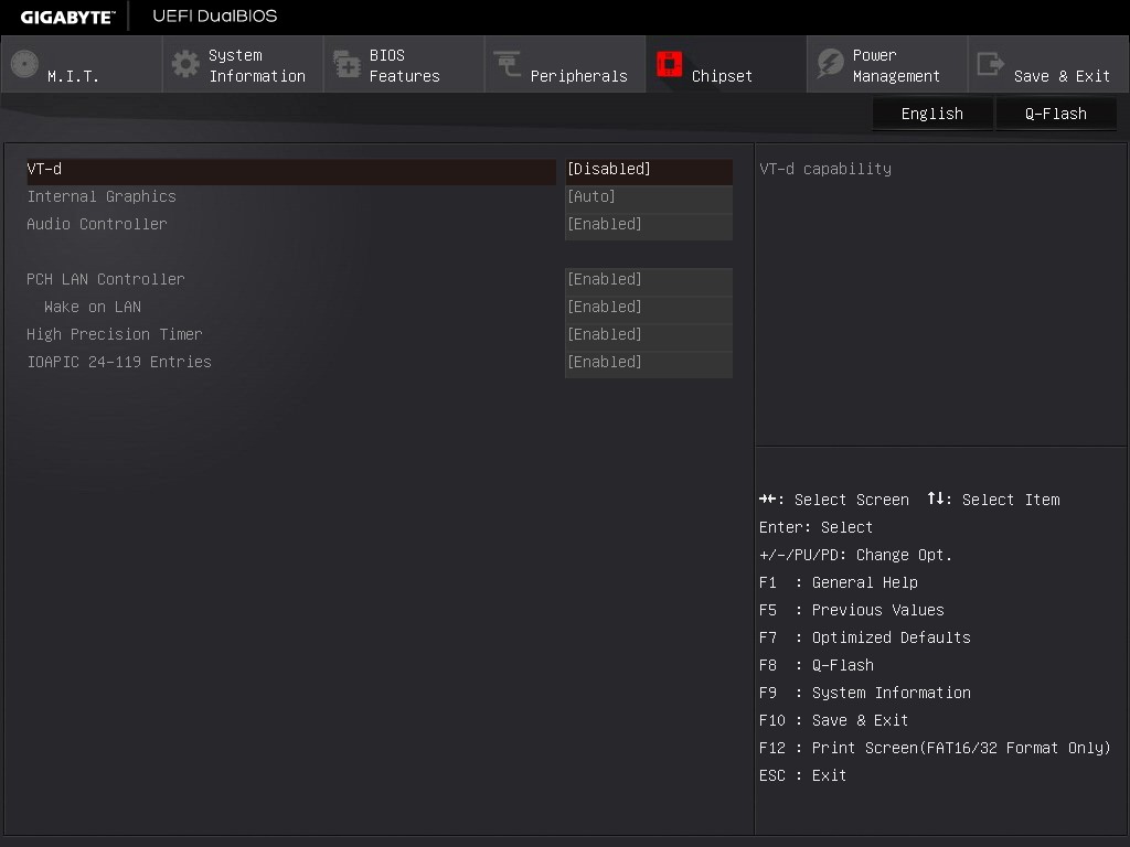
The Chipset tab is for integrated graphics and audio options, as well as virtualization through VT-d (which is disabled by default).
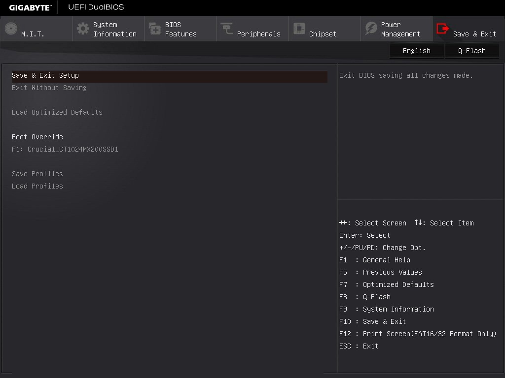
For boot override options, in order to boot from a single device for just one boot, these can be found in the Save and Exit menu.
A full series of images for this can be found in the BIOS gallery.


29 Comments
View All Comments
GoMoeJoe - Friday, February 19, 2016 - link
Any Z170 based mobo *that still uses a shared M.2 is unacceptable.Especially the way these clowns did it on this product ...
nehway0912 - Saturday, February 20, 2016 - link
There is a fw update for alpine ridge today. Can you retest the usb 3.1 performance with the lastest fw?jabber - Saturday, February 20, 2016 - link
Wake me up when I can buy a TB3 card for £10 and a TB3 caddy for around the same. No rush.garfieldalvin - Monday, February 22, 2016 - link
Any test perform on the TB3 port for read write data rate, displayport daisy chain with multi monitors?Zak - Friday, February 26, 2016 - link
Thunderbolt will never take off among consumers and enthusiasts due to cost and poor implementation in peripherals that make their price less attractive than USB. I have a TB2 dock and TB2 drive enclosure. USB3 in the dock maxes out at 350MB/s. SSDs mounted in the enclosure max out at 390/360MB/s R/W. All docks and all enclosures have this speed cutoff. And they're very expensive for what you get.olePigeon - Tuesday, April 12, 2016 - link
I don't think you quite understand what Thunderbolt is. Thunderbolt is essentially an external connector to your PCIe BUS. You don't compare it to USB. Sometimes it is USB because that's what you run on it. The advantage to Thunderbolt is that it is whatever you want it to be, including USB.Thunderbolt 3 currently combines either the USB 3 type C connector or DisplayPort 1.2 with PCIe in a single serial signal. This allows you to connect anything you would normally put into your PCIe slot. Many items can be found in the form of an adapter, such as ethernet, USB, SATA, etc.; others can be connected via an external PCIe slot such as video cards, audio cards, and more.
Thunderbolt doesn't compare to USB, it coexists.
WarlordBB - Monday, March 21, 2016 - link
With TB3 coming to several of Gigabytes Gaming boards, is this board worth it when the G1 is about the same price? Granted you get 2 TB3 instead of 1, but still:http://www.gigabyte.com/mb/thunderbolt3/overview
WarlordBB - Monday, March 21, 2016 - link
I meant the G7coldlogic - Tuesday, May 3, 2016 - link
Can anyone point me in the right direction to understand how TB3 passes video through from the GPU?