Semiconductors
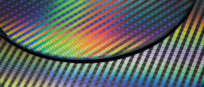
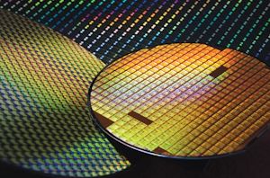
As announced last week by TSMC, later this year the company is set to start high-volume manufacturing on its N3P fabrication process, and this will be the company's most advanced node for a while. Next year things will get a bit more interesting as TSMC will have two process technologies that could actually compete against each other when they enter high-volume manufacturing (HVM) in the second half of 2025. Advertised PPA Improvements of New Process Technologies Data announced during conference calls, events, press briefings and press releases Compiled by AnandTech TSMC N3 vs N5 N3E vs N5 N3P vs N3E N3X vs N3P N2 vs N3E N2P vs N3E N2P vs N2 A16 vs N2P Power -25% -30% -34% -5% -10% -7%*** -25% -30% -30% -40% -5% -10% -15% -20% Performance +10% +15% +18% +5% +5% Fmax @1.2V** +10% +15% +15% +20% +5 +10% +8% +10% Density* ? 1.3x 1.04x 1.10x*** 1.15x 1.15x ? 1.07x 1.10x HVM Q4 2022 Q4 2023 H2 2024 H2 2025 H2 2025 H2 2026 H2 2026 H2 2026 *Chip density published by TSMC reflects 'mixed' chip density consisting of 50% logic, 30% SRAM, and 20% analog. **At the same area. ***At the same speed. The production nodes are N3X (3nm-class, extreme performance-focused) as well as N2 (2nm-class). TSMC says...
TSMC Offers a Peek at 'Global Gigafab' Process Replication Program
At its European Technology Symposium last week TSMC revealed some of the details about its Global Gigafab Manufacturing program, the company's strategy to replicate its manufacturing processes across its...
4 by Anton Shilov yesterday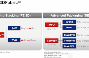
TSMC to Expand CoWoS Capacity by 60% Yearly Through 2026
Customer demand for AI and HPC processors is driving a much greater use of advanced packaging technologies, particularly TSMC's chip-on-wafer-on-substrate (CoWoS) services. As things stand, TSMC is just barely...
8 by Anton Shilov 2 days ago
TSMC Outlines Path to EUV Success: More Tools, More Wafers, & Best Pellicles In Industry
Although TSMC can't claim to be the first fab to use extreme UV (EUV) lithography – that title goes to Samsung – they do get to claim to be...
20 by Anton Shilov 6 days ago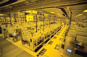
TSMC to Expand Specialty Capacity by 50%, Introduce 4nm N4e Low-Power Node
With all the new fabs being built in Germany and Japan, as well as the expansion of production capacity in China, TSMC is planning to extend its production capacity...
0 by Anton Shilov on 5/16/2024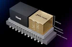
TSMC Readies Next-Gen HBM4 Base Dies, Built on 12nm and 5nm Nodes
Of the several major changes coming with HBM4 memory, one of the most immediate is the sheer width of the memory interface. With the fourth-generation memory standard moving from...
1 by Anton Shilov on 5/16/2024
TSMC: Performance-Optimized 3nm N3P Process on Track for Mass Production This Year
As part of the second leg of TSMC's spring technology symposium series, the company offered an update on the state of its 3nm-class processes, both current and future. Building...
21 by Anton Shilov on 5/15/2024
Samsung Tapes Out Its First 3nm Smartphone SoC, Gets A Boost From Synopsys AI-Enabled Tools
This week Samsung Electronics and Synopsys announced that Samsung has taped out its first mobile system-on-chip on Samsung Foundry's 3nm gate-all-around (GAA) process technology. The announcement, coming from electronic...
8 by Anton Shilov on 5/3/2024
Samsung Foundry Update: 2nm Unveil in June, Second-Gen SF3 3nm Hits Production This Year
As part of Samsung's Q1 earnings announcement, the company has outlined some of its foundry unit's key plans for the rest of the year. The company has confirmed that...
4 by Anton Shilov on 5/1/2024
TSMC Readies 8x Reticle Super Carrier Interposer For Next-Gen Chips Twice as Large As Today's
TSMC is no stranger to building big chips. Besides the ~800mm2 reticle limit of their normal logic processes, the company already produces even larger chips by fitting multiple dies...
6 by Anton Shilov on 4/30/2024
TSMC Jumps Into Silicon Photonics, Lays Out Roadmap For 12.8 Tbps COUPE On-Package Interconnect
Optical connectivity – and especially silicon photonics – is expected to become a crucial technology to enable connectivity for next-generation datacenters, particularly those designed HPC applications. With ever-increasing bandwidth...
9 by Anton Shilov on 4/26/2024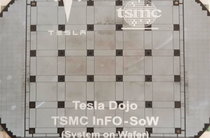
TSMC's System-on-Wafer Platform Goes 3D: CoW-SoW Stacks Up the Chips
TSMC has been offering its System-on-Wafer integration technology, InFO-SoW, since 2020. For now, only Cerebras and Tesla have developed wafer scale processor designs using it, as while they have...
2 by Anton Shilov on 4/26/2024
TSMC Preps Cheaper 4nm N4C Process For 2025, Aiming For 8.5% Cost Reduction
While the bulk of attention on TSMC is aimed at its leading-edge nodes, such as N3E and N2, loads of chips will continue to be made using more mature...
5 by Anton Shilov on 4/25/2024
TSMC 2nm Update: N2 In 2025, N2P Loses Backside Power, and NanoFlex Brings Optimal Cells
Taiwan Semiconductor Manufacturing Co. provided several important updates about its upcoming process technologies at its North American Technology Symposium 2024. At a high level, TSMC's 2 nm plans remain...
0 by Anton Shilov on 4/25/2024
TSMC's 1.6nm Technology Announced for Late 2026: A16 with "Super Power Rail" Backside Power
With the arrival of spring comes showers, flowers, and in the technology industry, TSMC's annual technology symposium series. With customers spread all around the world, the Taiwanese pure play...
18 by Anton Shilov on 4/25/2024
TSMC Posts Q1'24 Results: 3nm Revenue Share Drops Steeply, but HPC Share Rises
Taiwan Semiconductor Manufacturing Co. this week released its financial results for Q1 2024. Due to a rebound in demand for semiconductors, the company garned $18.87 billion in revenue for...
11 by Anton Shilov on 4/19/2024
ASML Patterns First Wafer Using High-NA EUV Tool, Ships Second High-NA Scanner
This week ASML is making two very important announcements related to their progress with high numerical aperature extreme ultraviolet lithography (High-NA EUV). First up, the company's High-NA EUV prototype...
13 by Anton Shilov on 4/18/2024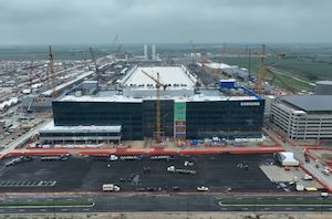
Samsung To Receive $6.4 Billion Under CHIPS Act to Build $40 Billion Fab in Texas
Samsung Electronics this week was awarded up to $6.4 billion from the U.S. government under the CHIPS and Science Act to build its new fab complex in Taylor, Texas...
5 by Anton Shilov on 4/16/2024
TSMC to Receive $6.6B Under US CHIPS Act, Set to Build 2nm Fab in Arizona
TSMC has entered into a preliminary agreement with the U.S. Department of Commerce, securing up to $6.6 billion in direct funding and access to up to $5 billion in...
23 by Anton Shilov on 4/8/2024
Rapidus to Get $3.9 Billion in Government Aid for 2nm, Multi-Chiplet Technologies
Rapidus, a Japan-based company developing 2nm process technology and aiming to commercialize it in 2027, will receive a huge government grant for its ongoing projects. The Japanese government will...
10 by Anton Shilov on 4/2/2024


