TSMC Readies 8x Reticle Super Carrier Interposer For Next-Gen Chips Twice as Large As Today's
by Anton Shilov on April 30, 2024 9:00 AM EST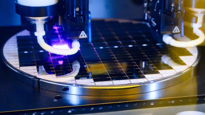
TSMC is no stranger to building big chips. Besides the ~800mm2 reticle limit of their normal logic processes, the company already produces even larger chips by fitting multiple dies on to a single silicon interposer, using their chip-on-wafer-on-substrate (CoWoS) technology. But even with current-gen CoWoS allowing for interposers up to 3.3x TSMC's reticle limit, TSMC plans to build bigger still in response to projected demand from the HPC and AI industries. To that end, as part of the company's North American Technology Symposium last week, TSMC announced that they are developing the means of building super-sized interposers that can reach over 8x the reticle limit.
TSMC's current-generation CoWoS technology allows for building interposers up to 2831 mm2 and the company is already seeing customers come in with designs that run up to those limits. Both AMD's Instinct MI300X accelerator and NVIDIA's forthcoming B200 accelerator are prime examples of this, as they pack huge logic chiplets (3D stacked in case of AMD's product) and eight HBM3/HBM3E memory stacks in total. The total space afforded by the interposer gives these processors formidable performance, but chip developers want to go more powerful still. And to get there as quickly as possible, they'll need to go bigger as well in order to incorporate more logic chiplets and more memory stacks.
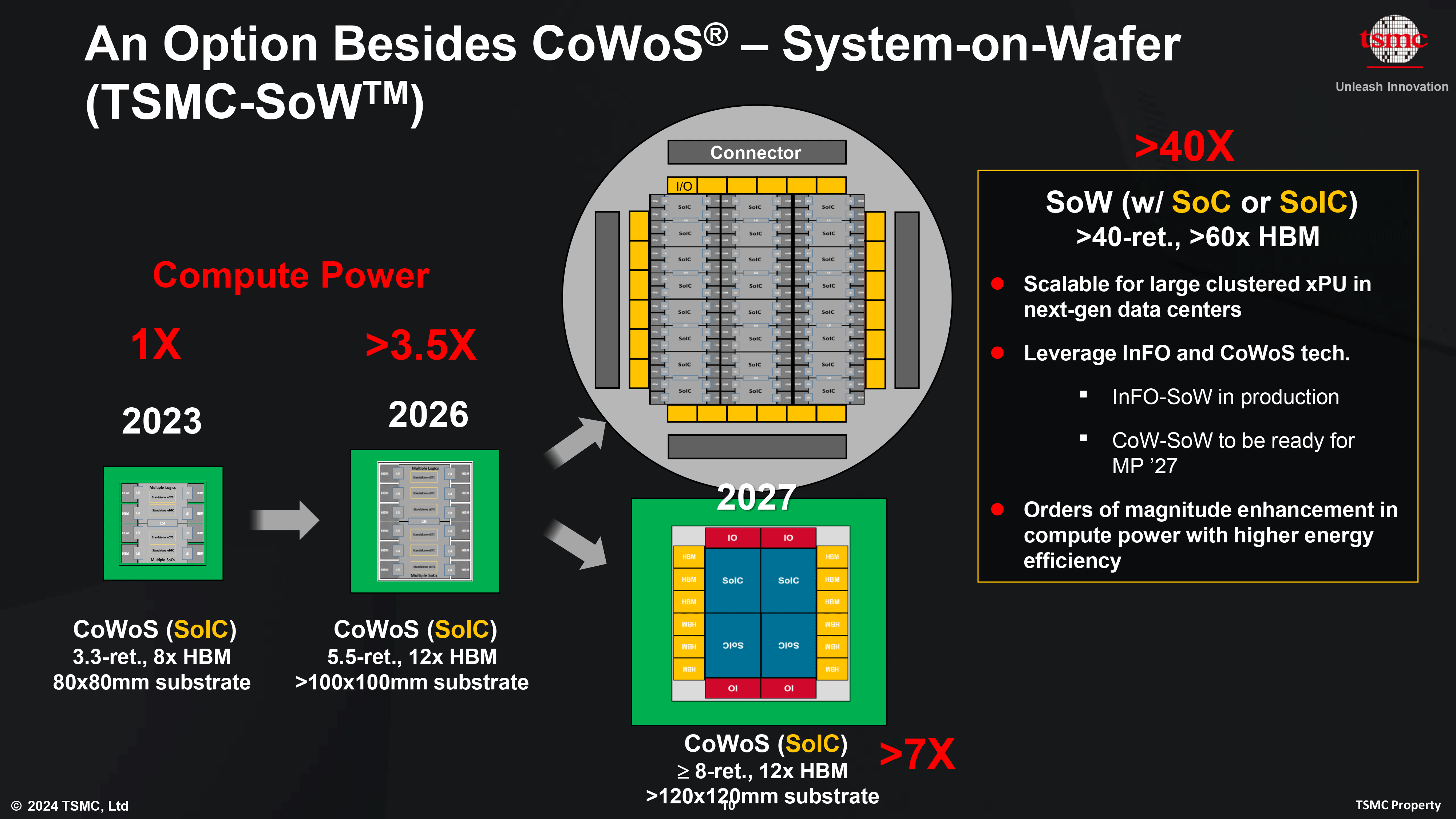
For their next-generation CoWoS product that's set to launch in 2026, TSMC plans to release CoWoS_L, which will offer a maximum interposer size of approximately 5.5 times that of a photomask, totaling 4719 mm² altogether. This next generation package will support up to 12 HBM memory stacks and will necessitate a larger substrate measuring at 100×100 mm. Coupled with process node improvements over the next few years, and TSMC expects chips based on this generation of CoWoS to offer better than 3.5x the compute performance of current-generation CoWoS chips.
Farther down the line, in 2027 TSMC intends introduce a version of CoWoS that allows for interposers up to 8 times larger than the reticle limit. This will offer an ample 6,864 mm² of space for chiplets on a substrate that measures 120×120 mm. TSMC envisions leveraging this technology for designs that integrate four stacked systems-on-integrated chips (SoICs), with 12 HBM4 memory stacks and extra I/O dies. TSMC roughly projects that this will enable chip designers to once again double performance, producing chips that surpass 7x the performance of current-generation chips.
Of course, building such large chips will come with its own set of consequences, above and beyond what TSMC will have to deal with. Enabling chip designers to build such grand processors is going to impact system design, as well as how datacenters accommodate these systems. TSMC's 100×100mm substrate will be riding right up to the limit of the OAM 2.0 form factor, whose modules measure 102×165mm to begin with. And if that generation of CoWoS doesn't break the current OAM form factor, then 120×120mm chips certainly will. And, of course, all of that extra silicon requires additional power and cooling, which is why we're already seeing hardware vendors prepare for how to cool multi-kilowatt chips by investigating liquid and immersion cooling.
Ultimately, even if Moore's Law has slowed to a crawl in terms of delivering transistor density improvements, CoWoS offers an out for producing chips with an ever-larger number of transistors. So with TSMC set to offer interposers and substrates with over twice the area of today's solutions, big chips intended for HPC systems are only going to continue to grow in both performance and size.
Related Reading
- TSMC's 1.6nm Technology Announced for Late 2026: A16 with "Super Power Rail" Backside Power
- TSMC 2nm Update: N2 In 2025, N2P Loses Backside Power, and NanoFlex Brings Optimal Cells
- TSMC Preps Cheaper 4nm N4C Process For 2025, Aiming For 8.5% Cost Reduction
- TSMC's System-on-Wafer Platform Goes 3D: CoW-SoW Stacks Up the Chips
- TSMC Jumps Into Silicon Photonics, Lays Out Roadmap For 12.8 Tbps COUPE On-Package Interconnect


6 Comments
View All Comments
Dante Verizon - Tuesday, April 30, 2024 - link
This does not solve the problem of skyrocketing prices due to the slowdown in manufacturing processes, complexity and lack of competition in the sector Replymukiex - Tuesday, April 30, 2024 - link
Nor does it attempt to. That would happen via competition or just a glut of manufacturing capacity. The former is stalled with a potential for resurgence if Samsung's Nintendo deal goes well, and the latter comes down to whether TSMC can pivot in countries outside of Taiwan. ReplyKevin G - Wednesday, May 1, 2024 - link
This doesn't address that but the way packaging technology works offers an alternative path to increasing performance. Instead of cramming more transistors into an similar area based upon new manufacturing process nodes, this enables designers to stich multiple pieces of silicon together to get the same amount of transistors for a design over a larger silicon area. There are certainly trade offs, power consumption and packaging yields being the big ones. Cost is a harder one to determine as new nodes have significantly higher costs associated with them but so does this packaging technology.The real interesting aspect is power consumption and temperatures. Newer nodes are not offering as great of power savings as they used to. Combine that by scaling up designs to use more functional units over more area but at reduced clocks/voltage to normalize performance, the power consumption could be lower with these new packaging technologies. Temperatures would arguably be lower as well as the power draw would be spread across more area. The downside to this approach is that it does cost more due to additional silicon where as higher voltages/clocks are 'free' in that sense (designs due need more complex VRM for power delivery, better heat sink etc.). Reply
wrosecrans - Tuesday, April 30, 2024 - link
"Reticle super carrier interposer" definitely sounds like a sequence of words I've heard in a reeeally low budget sci fi series that didn't know what any of those words meant. Possibly some sort of Canadian-European coproduction where half the cast had learned their lines phonetically.But seriously, bigger chips is interesting. The industry is sort of divided between "Is there anything else we can throw into the SOC to use up some of our giant transistor budget we don't know what to do with?" and "Throw infinity more low precision floating point units in because our AI/Graphics problems are sufficiently parallelizable that we'd gladly consume 1,000x the area of current chips without blinking." I wonder if the economics really work out for 2x bigger chips today the way they have for most of the history of Moore's law. If you could fab a 2x bigger chip in the 90's, you were obviously going to be instantly buried in customers because everybody knew exactly what they'd do with an extra million transistors and was just waiting for the hardware to get there. Today, "more GPU, but it costs over 2X as much because it's 2X the silicon and the fab process is more complex, and latencies aren't improved - only compute throughput" may not be as much of a slam dunk. Reply
Rοb - Saturday, May 4, 2024 - link
In US-terms it's 'butts in the seats'.Using UCIe-Advanced based die-to-die connectivity latency is expected to be under 2ns, and pJ/bit better than 40x improved compared to PCIe Gen5.
Putting everything that works together on one chip and what doesn't (or can be split) on seperate chiplets (using silicon made on different nodes) not only is effective use of the area but cost effective from a manufacturing perspective.
2x the cost for 2x the performance isn't a loss, other gains are the power efficiency and the size; both of which are significant for day to day operating costs. A new motherboard with a new chip that can replace a system that took up 3-4x as much space under the same power budget is a huge savings, a slam dunk with a swish. Reply
MoogleW - Thursday, May 2, 2024 - link
So reticle limit will be halved in the future but chips can be stitched up to 8X reticle limit so about 4 of todays reticle limit size chips together. Interesting Reply