CPUs
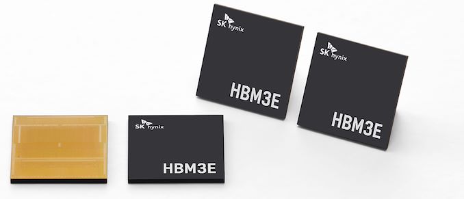
SK hynix and TSMC announced early on Friday that they had signed a memorandum of understanding to collaborate on developing the next-generation HBM4 memory and advanced packaging technology. The initiative is designed to speed up the adoption of HBM4 memory and solidify SK hynix's and TSMC's leading positions in high-bandwidth memory and advanced processor applications. The primary focus of SK hynix's and TSMC's initial efforts will be to enhance the performance of the HBM4 stack's base die, which (if we put it very simply) acts like an ultra-wide interface between memory devices and host processors. With HBM4, SK hynix plans to use one of TSMC's advanced logic process technologies to build base dies to pack additional features and I/O pins within the confines of existing...
Intel Releases Atom D2500 and D2700 Processors
Back in April, we reported the specifications of Intel's upcoming Cedar Trail platform. On Sunday, Intel quietly updated their CPU price list with two new SKUs: Atom D2500 and...
20 by Kristian Vättö on 9/27/2011
AMD Announces Next Financial Analyst Day: February 2012
For the past three years AMD has held an annual Financial Analyst Day at its HQ in Sunnyvale, CA in November. That was the case for 2008, 2009 and...
17 by Anand Lal Shimpi on 9/22/2011
Products Group GM Rick Bergman Leaves AMD
For the first time in years AMD is set to really start executing on the CPU side. Although Bulldozer has faced significant delays, Brazos and Llano were both warmly...
11 by Anand Lal Shimpi on 9/22/2011A Look Into Sandy Bridge-E Overclocking
Note: Most Sandy Bridge-E information is currently under embargo, but the information below comes from Bit-tech's article detailing SNB-E overclocking. Sandy Bridge-E release is getting closer and closer all the...
11 by Kristian Vättö on 9/21/2011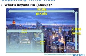
Ivy Bridge GPU to Support Resolutions of up to 4096x4096
Thanks VR-Zone for the image! IDF 2011 ended on last Thursday but there is still lots of data showing up because sites are processing the data they have gathered. VR-Zone...
33 by Kristian Vättö on 9/19/2011
Intel's Ivy Bridge Architecture Exposed
Five years ago Intel announced its ambitious tick-tock release cadence. We were doubtful that Intel could pull off such an aggressive schedule but with the exception of missing a...
98 by Anand Lal Shimpi on 9/17/2011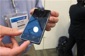
There Will Be Two 32nm Atom SoCs in 2012: Medfield and One Other
Intel did a good job of showing off what it promises to deliver with Medfield at IDF: a reasonably looking smartphone and tablet built around the platform. As a...
7 by Anand Lal Shimpi on 9/17/2011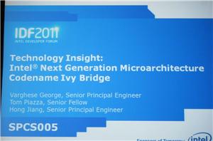
IDF 2011 Recap and Announcing Pipeline
A little over a month ago we quietly introduced a new section to AnandTech called Pipeline. You'll find it in the right hand column of the site where we...
19 by Anand Lal Shimpi on 9/16/2011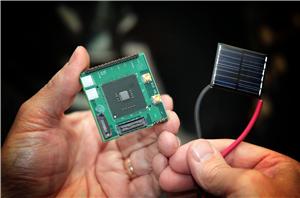
Rattner Shows off Near Threshold Voltage Intel Architecture CPU
Most modern day Intel CPUs run at or above 1V depending on clock speed. For years we had seen decreasing core voltages as Intel transitioned to lower power manufacturing...
21 by Anand Lal Shimpi on 9/15/2011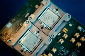
Intel and Micron Develop Hybrid Memory Cube, Stacked DRAM is Coming
During the final keynote of IDF, Intel's Justin Rattner demonstrated a new stacked DRAM technology called the Hybrid Memory Cube (HMC). The need is clear: if CPU performance is...
19 by Anand Lal Shimpi on 9/15/2011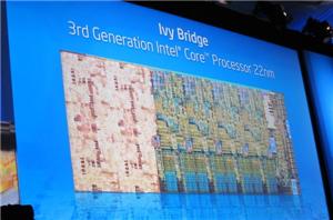
Counting Transistors: Why 1.16B and 995M Are Both Correct
Yesterday we published Ivy Bridge's transistor count as 1.48 billion. It turns out that was wrong as Intel's Mooly Eden accidentally read the B in billion as an 8...
26 by Anand Lal Shimpi on 9/15/2011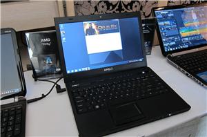
Look Out Bulldozer, Here Comes Trinity: AMD's 2012 Demo on Video at IDF
AMD's Bulldozer CPU is on the verge of being released. Sever markets will see the CPU soon, while desktop customers will have to wait until Q4 (which is only...
33 by Anand Lal Shimpi on 9/14/2011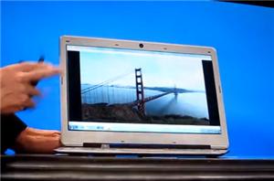
Ultrabooks on Video: Rapid Start & Smart Connect
Ultrabooks are a three year play for the industry and it's clear that software & features are going to be a major part of the evolution. Intel showed off...
2 by Anand Lal Shimpi on 9/14/2011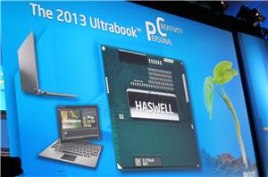
First Shot of Haswell, Working Demo at IDF
What you're looking at above is the first shot of Haswell, Intel's 2013 Core microarchitecture that replaces Ivy Bridge. Haswell is designed for a 10 - 20W range of...
4 by Anand Lal Shimpi on 9/14/2011
Ivy Bridge: 1.4B Transistors
Intel's Mooly Eden just disclosed Ivy Bridge's transistor count to a captive audience at IDF this morning: 1.4 billion transistors. That's presumably for the quad-core version compared to 1.16B...
16 by Anand Lal Shimpi on 9/14/2011
X79 Motherboards from Gigabyte & MSI at IDF 2011
IDF isn't a traditional trade show in the sense that the majority of the show isn't built around a wide open show floor with tons of booths and product...
16 by Anand Lal Shimpi on 9/13/2011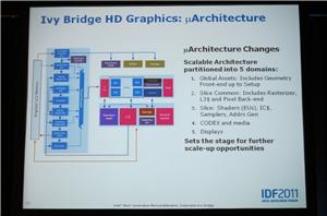
And Now: Ivy Bridge GPU Architectures Detailed
We just finished going over the GPU portion of Ivy Bridge in Intel's IVB tech session. If you're interested, the slides are below.
12 by Anand Lal Shimpi on 9/13/2011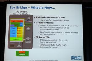
Ivy Bridge CPU Architecture Details Revealed
We're still working on our deep dive on Intel's Ivy Bridge architecture but for those who are interested the slide deck that Intel just presented is in the gallery...
7 by Anand Lal Shimpi on 9/13/2011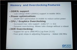
Ivy Bridge Overclocking: Ratio Changes Without Reboot, More Ratios and DDR3-2800
Ivy Bridge has three new features for overclocking: The max CPU ratio is now 63x up from 57x You can now adjust CPU ratios without a reboot, just via a register...
6 by Anand Lal Shimpi on 9/13/2011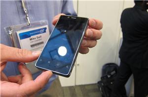
Intel's Medfield Gingerbread Smartphone Reference Platform
Earlier this morning Paul Otellini showed off Intel's Android smartphone reference platform running a version of Gingerbread. We just got up close and personal with the device as you...
11 by Anand Lal Shimpi on 9/13/2011


